Advances in Light Sources: ArF immersion lithography: Understanding light source performance
TED CACOURIS, PAOLO ALAGNA, OMAR ZURITA, WILL CONLEY, and GREG RECHSTEINER
Consumer electronics—particularly smartphones—are a key market segment driving demand for advanced chip technology. Mobile-device manufacturers are continually exploring ways to increase processor functionality and memory, all within a smaller form factor, with longer battery life, and at a lower price point to gain a competitive advantage.
Photolithography is one of the primary technologies that enable these device performance advancements by shrinking chip geometries. However, the increasing cost and complexity associated with advanced photolithography techniques is also driving the need for chipmakers to further maximize the productivity of photolithographic tools, such as scanners, and improve yield to support the economics of the consumer market.
By using deep-ultraviolet argon fluoride (DUV ArF) excimer-laser immersion lithography at a 193 nm wavelength, engineers have been able to extend device scaling through techniques such as double- and multipatterning, methods that rely on two or more exposures and masks for each layer to deliver the desired patterns at the required resolution and density. As a result, multi-patterning, which helps to produce features well below the diffraction limit of 193 nm light, is now planned to be used for producing 10-nm-node chip designs.
Additionally, techniques such as source-mask optimization (SMO) and optical proximity correction (OPC) are part of the lithographer's toolbox to faithfully reproduce the chip designer's patterns onto silicon. OPC prevents patterning distortions in the printed feature by designing countermeasures in the mask. Multi-patterning, SMO, and OPC processes increase lithography cost and complexity, requiring further improvements in process control and stability to maximize yield.1-3
The optimal printability for multiple patterning-based logic devices is also driven by complex process factors, such as photoresist, exposure tool, and mask-related error performance levels, as well as light source performance. It has been widely demonstrated that changes in the light source's narrow spectral bandwidth can lead to significant changes in on-wafer patterning due to image contrast changes.4-8
All together, these new approaches create aggressive process windows and yield specifications, and place tighter requirements on exposure tool performance, especially focus budgets (the depth of focus required to pattern an image based on the tool control capability). In turn, they result in complicated systems and the need for further studies to identify areas of opportunity to improve performance.
Process characterization studies
While the lithography exposure tool, or scanner, has been extensively characterized to understand how the various input parameters (focus, dose, overlay, and so on) can affect on-wafer printing performance (contrast, resolution, etc.), fewer studies have been dedicated specifically to the light source.
To better understand the impact of light source performance (bandwidth, wavelength, and energy) on patterning, new novel computational and experimental approaches have been developed to enable process characterization studies.9-11 Using these new data-driven methodologies, chipmakers can more easily study and identify critical light source performance factors that can impact patterning results.
To this end, Cymer developed advanced techniques for modulating light source optical performance levels to enhance the characterization of specific patterning layer responses. Optical modulation methods can enable field-level modulation of bandwidth, wavelength, and energy stability across a wafer exposure, providing results that are not confounded with wafer-to-wafer variability.
Expanding on the characteristic process window for the lithography steps, which includes exposure latitude, dose, and depth-of-focus parameters, Cymer's Will Conley and others proposed the concept of a "variability window" to assess the impact E95 bandwidth has on a representative 14-nm-node contact patterning process.8 A figure of merit for the spectral profile, E95 is defined as the width that contains 95% of the integrated spectral intensity. By applying the variability window approach across documented scanner dose and focus control ranges, chipmakers are able to determine the minimum feature size, or critical dimension (CD), response due to E95 bandwidth variability.
Computational details and results
Recently, we performed simulations based on the variability window concept to study the impact that E95 bandwidth has on 10-nm-node Metal 1 layer patterning.11 While not all printed features are sensitive to process variations, there are critical patterning geometries that are very susceptible to process variations and are classified as "hot spots" since they can result in poor patterning results. We were most interested in these specific hot spots and their response to bandwidth variations.
To study the E95 bandwidth impact on 10-nm-node Metal 1 layer patterning, we used a popular lithography simulation tool, HyperLith v7 from Panoramic Technology (Berkeley, CA), to simulate the patterning response to bandwidth for a 38 nm contact hole structure. Detailed descriptions of the simulation were reported in the 2015 SPIE paper by Conley et al.8
Most ArF immersion light sources have a target bandwidth of 300 fm E95 with a typical variation of 10–20%. This study used a bandwidth variation of 300 fm (+75/-25 fm) and focus variation of ±15 nm, based on existing known scanner specifications; no dose variations were considered.
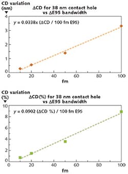
By using these computational methods and techniques, they determined pattern-specific responses of 14-nm-node (N14) and below logic structures to E95 bandwidth performance levels. After conducting simulations using a variability window methodology (with known scanner dose and focus variations, and known E95 bandwidth variations in current ArF light sources), results predicted a ~3 nm change per 100 fm of E95 bandwidth change—nearly a 10% change in CD across the studied E95 bandwidth range (see Fig. 1).
Experimental details and results
To confirm the simulation results, Cymer and imec (Leuven, Belgium) printed a 10-nm-node Metal 1 pattern using Cymer's advanced technique for modulating light source optical parameters. Data was collected using an ASML NXT:1950i ArF immersion scanner and a Cymer XLR 660ix light source with Cymer's SmartPulse data product. The imaging conditions were a numerical aperture (NA) of 1.35 and xy polarization (which is oriented at 45° from both x and y) using a custom (freeform) illumination condition and a negative tone develop (NTD) process. This study explored E95 bandwidth settings of 300, 310, 400, 450, and 490 fm.
Cymer and imec selected six hot spot (HS) structures based on the complexity of the OPC model of the test vehicle to study the impact E95 bandwidth modulation had on patterning performance on a structure-specific basis. They also used a line-space structure as the anchor, or reference, feature to target each wafer exposure. The CD targets for each hot spot varied between 43 and 47 nm, with each hot spot having a CD tolerance of ±3 nm.
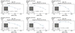
By using wafer-to-wafer E95 bandwidth modulation, the investigators studied the response of the hot spot structures. A quadratic response of depth of focus (DOF) to bandwidth was observed for most of the hot-spot structures sampled (see Fig. 2). Each of the six selected hot spots exhibited different degrees of sensitivity to E95 modulation.Cymer and imec also determined the impact of E95 on the lithography process window for each hot spot in terms of change in depth of focus, or Δ(DOF), vs. E95 bandwidth. One of the structures, hot spot HS_01, exhibited the largest shift in DOF vs. bandwidth, measuring 30 nm per 100 fm of E95.
While DOF is a key metric for characterizing a process, additional performance metrics must be studied to assess the overall impact of E95 bandwidth on process capability. An increase in E95 bandwidth degrades not only process window performance, but also CD uniformity (CDU), line width roughness (LWR), and other key performance metrics.
Cymer and imec determined CDU responses were structure specific, with some hot spots showing limited, if any, response to E95 bandwidth modulation. Line width roughness measurements started to show an increase in roughness between 0.5 and 1 nm at 400 fm E95 bandwidth and above. Line-end shortening in a line-space matrix also showed a sensitivity of 2.5 nm CD/10 fm E95.
In summary, the study found that E95 bandwidth variation greater than ±10 fm induced patterning changes (CD) that were beginning to impact 10-nm logic-node features. Maintaining tight bandwidth control within these limits would eliminate bandwidth as a source of variation for the printed features, thus defining one of the key light source requirements for this device generation.
Conclusions
By using these computational and experimental methods, chipmakers are able to more effectively characterize the impact of light source parameters such as E95 bandwidth on advanced lithography processes. This work has extended the understanding of all the variables that contribute to the successful printing of leading-edge chip designs, providing additional tools to further optimize ArF immersion lithography and guiding the requirements of the lithography equipment. Lower variability of the light source bandwidth has been identified as one of the requirements, which is now achievable on the latest-generation ArF immersion light source, Cymer's XLR 700ix, enabling higher yields and more cost-effective solutions.
ACKNOWLEDGEMENT
SmartPulse is a registered trademark of Cymer.
REFERENCES
1. P. Wennink, "Creating value for all stakeholders," ASML Investor Day (2014).
2. See http://www.itrs.net.
3. H. Egashira et al., "Immersion scanners enabling 10 nm half pitch production and beyond," Proc. SPIE, 9052, Optical Microlithography XXVII, 90521F-1 (2014).
4. U. Iessi et al., "Laser bandwidth effect on overlay budget and imaging for the 45 nm and 32nm technology nodes with immersion lithography," Proc. SPIE, 7973, Optical Microlithography XXIV, 797328.
5. N. Seong et al., "Analysis of the effect of laser bandwidth on imaging of memory patterns," Proc. SPIE, 7140, Lithography Asia, 714042 (2008).
6. P. De Bisschop et al. J. Micro. Nanolithogr. MEMS MOEMS, 7, 3 (2008).
7. N. Seong et al., "Analysis of the effect of laser bandwidth on imaging of memory patterns," Proc. SPIE, 7140, Lithography Asia, 714042 (2008).
8. W. Conley et al., "Impact of bandwidth on contrast sensitive structures for low k1 lithography," Proc. SPIE, 9526, Optical Microlithography XXVIII, 9526-07 (2015).
9. P. Alagna et al., "Lithography imaging control by enhanced monitoring of light source performance," Proc. SPIE, 8683, Optical Microlithography XXVI, 86830S (2013).
10. P. Alagna et al., "Improving On-Wafer CD Correlation Analysis Using Advanced Diagnostics and Across-Wafer Light-Source Monitoring," Proc. SPIE, 9052, Optical Microlithography XXVII, 905228 (2014).
11. P. Alagna et al., "Optimum ArF laser bandwidth for 10 nm node logic imaging performance," Proc. SPIE, 9525, Optical Microlithography XXVIII, 9525-08 (2015).
Ted Cacouris, Omar Zurita, Will Conley, and Greg Rechtsteiner are at Cymer, San Diego, CA, while Paolo Alagna is at Cymer Europe; e-mail: [email protected]; www.cymer.com.

