Increasingly, aspheric components are being specified in optical designs. What once was used only in ultraprecise (in other words, very expensive) systems has now become relatively commonplace. There are many reasons for this, from developments in manufacturing, metrology, and materials to advances in computing power and optical-modeling software. Nowhere is this phenomenon more evident than in the design of infrared (IR) optical systems, where aspheric elements are as common as spherical ones. But as IR systems transition from the domain of government-funded development efforts to commercially viable products, much consideration needs to be given to how aspheres are specified.
Material choice is the first step in defining the manufacturing method used to produce the asphere. Thus, understanding the benefits and limitations of the various manufacturing methods (which include single-point diamond turning, molding, subaperture polishing, and magnetorheological finishing) are critical factors in the design process. Fortunately for the designer, strides are being made not only in manufacturing methods but also material availability, resulting in fewer compromises, more cost-effective components, and, most important, manufacturable geometries that were not imaginable a few years ago.
Characteristics of IR materials
First, it is important to examine a few of the intricacies that differentiate IR aspheres from their visible counterparts. By and large, the materials used to produce aspheres in the IR exhibit very low dispersion and very high indices of refraction; designers are wise to use both of these characteristics to their advantage.
While the high index of refraction can produce some throughput challenges (overcome with the use of antireflection coatings), it also allows for the design of high-numerical-aperture (NA) lenses. High NAs mean increased light gathering and, in the case of aspheres designed to operate with diffraction-limited performance, small spot sizes. However, operating at such high NAs is not without challenges. Typically in the IR, a lens with a high NA will be operating over a wide acceptance angle.
At wide angles, deficiencies in surface figure and finish can cause scatter and affect the image quality of the optical system.1 From a roughness standpoint, the angle of scattered light can be directly calculated using the grating equation: the shorter the spatial period, the higher the deflected angle. The amplitude of the scatter, likewise, is easily calculated. Luckily, high-index materials and long wavelengths are surprisingly insensitive to scatter (see Table 1). An optical system consisting of two germanium (Ge) elements designed to operate at a wavelength of 4 μm, for instance, could have a per-surface roughness specification of 5 nm and only suffer just over 0.7% total loss due to scatter.
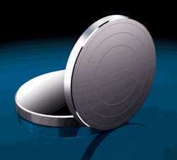
The introduction of actual surface-grating features is common in the IR. Diffractive features exhibit the interesting property of negative dispersion: The introduction of a grating onto an asphere surface provides chromatic aberration correction. The low sensitivity to scatter, coupled with the low dispersion of common IR materials such as Ge and zinc selenide, means this chromatic-aberration correction is relatively easy to achieve on a single-element asphere. Consider, for instance, a color-corrected Ge asphere with a 25 mm clear aperture and an NA of 0.63 designed to operate in the 3–5 μm region (see Table 2 and photo). To fully correct for chromatic aberration, 17 rings are necessary. A similar asphere, designed with Zeonex E48R (nd = 1.531) and color-corrected for the visible spectrum, requires 425 rings in that same 25 mm aperture.
Manufacturing methods
With these additional tools in the toolbox, the designer needs to determine how the asphere will be manufactured. Three common methods for asphere manufacturing are single-point diamond turning (SPDT), subaperture polishing, and precision molding.
Single-point diamond turning has a greater than 30 year history of producing aspheres, dating back to the 1970s and the emergence of IR night-vision systems. A computer-numerical-controlled (CNC) SPDT lathe typically sits atop a granite base, finished to micrometer-level quality, and supported by air suspension. The cutting tool is moved with picometer precision by a combination of electric motors and piezoelectric actuators. The machined component is attached to an air chuck, centered manually using a micrometer, and machined from a list of coordinates generated directly from a CAD model. The final surface is achieved with a series of cutting passes of decreasing depth.
With advances in controls, feedback systems, and drive systems, today’s single-point diamond-turning machines are able to produce impressive optical quality. Today, state-of-the-art equipment is able to produce parts with peak-to-valley surface figures on the order of 100 nm and surface textures on the order of 2 nm. Beyond optical characteristics, SPDT surfaces provide some mechanical advantages as well. Chief among them is the fact that the edge is turned at the same time as the aspheric surface, assuring registration of the mechanical and optical axes. Therefore, for systems requiring precise centering or “snap-together” construction, a diamond-turned surface is hard to beat.
Material selection is a major issue for diamond turning. In general, ferrous materials are not readily machinable because the carbon in the diamond tool chemically reacts with the substrate, leading to tool damage and dulling after short cut lengths. When an optical design calls for silicon or silicon-based glass, beryllium, steel, or other ferrous materials, alternative techniques should be considered. However, most non-ferrous alloys, such as aluminum, gold, and brass, as well as Ge, zinc sulfide, zinc selenide, calcium fluoride, gallium arsenide, and a variety of plastics are well suited to this technique.
Single-point diamond turning is also a critical enabling technology for another IR aspheric manufacturing technique—precision molding. In the IR, molding is the newest, and likely least utilized, of the manufacturing technologies for designers to consider.
Molding has many advantages, chief among them being the scaling of cost and capacity to meet high volume needs. In fact, molding is the best choice for most high-volume production aspheres, as multicavity tools can press replicated lenses much more quickly, with relatively little compromise in optical quality, compared to diamond-turning or polishing techniques. However, current molding technology requires the transformation temperature (Tg) of the lens material to be less than approximately 800°C, and ideally to be less than 400°C, eliminating many common IR materials.
The lack of availability of a robust selection of materials along the Abbe diagram is the major drawback to IR molding. Today, a small selection of AMTIR variety glasses from Amorphous Materials (Garland, TX), the UVIR material from IRphotonics (Hamden, CT), and the IG glasses from Vitron Spezialwerkstoffe (Jena, Germany) are the only materials an optical designer has to choose from. Fortunately, much research is ongoing in characterizing the performance of moldable chalcogenide materials and formulating new materials.
An additional issue with molding is the current size limitation associated with the process. State-of-the-art equipment can mold diameters up to 75 mm, but practical considerations arising from heating and cooling gradients and preform geometries typically keep molding from being practical for sizes above a few tens of millimeters.
For the most complex geometries or for larger optics, subaperture polishing is most likely the best solution. While diamond turning and molding is typically restricted to rotationally symmetric aspheric symmetries, subaperture polishing is able to readily handle free-form solutions. This technique polishes aspheres on a single CNC controlled spindle, spinning the lens at high speed while a small contact area polishing tool is translated from the edge of the lens to the center. The precision control over the location of the tool allows the aspheric shape to be polished into the lens. In typical equipment available today, that precision is on the order of 100 nm, depending on geometry.
Further correction can be accomplished through magnetorheological finishing of the surface. Just about any material can be polished using this technique—certainly all commonly available glasses, IR crystalline materials, and ceramics.
REFERENCE
1. J.R. Harvey and A. Kothka, “Scattering effects from residual optical fabrication errors,” Proc. SPIE, 2576, 155 (1995).
About the Author
Gregg Fales
Senior Product Line Manager, Edmund Optics
Gregg Fales is senior product line manager, both at Edmund Optics (Barrington, NJ).


