ZEISS enters semiconductor process control market
ZEISS (Oberkochen, Germany) is fueling its growth strategy by expanding into a new market in the semiconductor industry. Through its new Process Control Solutions (PCS) business unit in Pleasanton, CA, the company will leverage its core technology solutions and partnerships to address a range of special needs for semiconductor customers. The new business unit will be part of the ZEISS Semiconductor Manufacturing Technology (SMT) business group and draw on long-standing innovations in microscopy that ZEISS is well known for.
"We see a strong trend in semiconductors toward complex 3D chip structures and new materials," said Karl Lamprecht, head of SMT business group. "As development cycles lengthen and R&D costs climb, the role of metrology changes. Our customers need effective process control solutions delivering integrated, actionable information that speeds time to problem resolution and time to production. ZEISS has the technology and expertise to fulfill these requirements."
RELATED ARTICLE: Veeco completes Ultratech acquisition to grow LED and semiconductor processing portfolio
With shrinking structure sizes, ever more sophisticated designs and hundreds of individual working steps, the semiconductor manufacturing workflow has become increasingly challenging. Fast and cost-effective process control solutions play a key role in ensuring the functioning of semiconductor devices. ZEISS is already a leading solutions provider in the semiconductor industry with its portfolio of lithography optics and mask metrology and repair solutions, and is now bringing its decades of semiconductor equipment experience into the market for semiconductor process control solutions.
The PCS business unit will utilize and expand upon ZEISS's existing portfolio of products, including its core proprietary microscopy technologies, to penetrate the semiconductor lab and fab space. Key products to be deployed include ZEISS's electron microscope products ZEISS Crossbeam and ZEISS MultiSEM, ion-beam microscope ZEISS ORION NanoFab, as well as the ZEISS Xradia Versa and ZEISS Xradia Ultra non-destructive 3D X-ray microscope systems. Process control solutions will be offered across the spectrum of semiconductor manufacturing process steps, including front end of line (FEOL), back end of line (BEOL), packaging, and assembly.
"Our process control solutions offer comprehensive structural, chemical and electrical information. By creating a single window into ZEISS for our semiconductor customers, we will enable them to address their process control challenges with seamlessly integrated technologies, helping them get their products to market faster," said Raj Jammy, Head of ZEISS PCS business unit, headquartered in Pleasanton, CA.
Jammy, who has more than 20 years of extensive semiconductor industry experience, joined ZEISS in February 2016. After obtaining a PhD in electrical engineering from Northwestern University, he started his career at IBM in New York and held subsequent leading positions at SEMATECH and Intermolecular. Jammy and his team will collaborate closely with global customers to address semiconductor inspection and review, failure analysis, defect detection, 3D tomography, and process characterization and analysis.
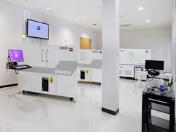
To aid in this effort, the new ZEISS Customer Center Bay Area was opened in Pleasanton on June 15, 2017. Located near the heart of Silicon Valley, this facility joins ZEISS's global network of customer centers in making the company's portfolio of optical, ion, electron and X-ray microscopy offerings available for demonstrations, application development and training.
SOURCE: ZEISS; https://www.zeiss.com/corporate/int/zeiss-corporate-newsroom/news/press-releases.html?id=process-control-solutions_2017
About the Author

Gail Overton
Senior Editor (2004-2020)
Gail has more than 30 years of engineering, marketing, product management, and editorial experience in the photonics and optical communications industry. Before joining the staff at Laser Focus World in 2004, she held many product management and product marketing roles in the fiber-optics industry, most notably at Hughes (El Segundo, CA), GTE Labs (Waltham, MA), Corning (Corning, NY), Photon Kinetics (Beaverton, OR), and Newport Corporation (Irvine, CA). During her marketing career, Gail published articles in WDM Solutions and Sensors magazine and traveled internationally to conduct product and sales training. Gail received her BS degree in physics, with an emphasis in optics, from San Diego State University in San Diego, CA in May 1986.