IBM uses EUV lithography to reach 5 nm semiconductor node
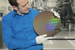
IBM (NYSE: IBM; Albany, NY) and its Research Alliance partners GLOBALFOUNDRIES, Samsung, and equipment suppliers have developed a process to build silicon nanosheet transistors that will enable 5 nm semiconductor chips. In less than two years since developing a 7 nm test node chip with 20 billion transistors, scientists have paved the way for 30 billion switches on a fingernail-sized chip.
RELATED ARTICLE: TRUMPF invests nearly $80M in EUV laser facility in Ditzingen
The resulting increase in performance will help accelerate cognitive computing, the Internet of Things (IoT), and other data-intensive applications delivered in the cloud. The power savings could also mean that the batteries in smartphones and other mobile products could last two to three times longer than today’s devices, before needing to be charged.
Scientists working as part of the IBM-led Research Alliance at the SUNY Polytechnic Institute Colleges of Nanoscale Science and Engineering's NanoTech Complex in Albany, NY achieved the breakthrough by using stacks of silicon nanosheets as the device structure of the transistor, instead of the standard FinFET architecture, which is the blueprint for the semiconductor industry up through 7nm node technology.
"For business and society to meet the demands of cognitive and cloud computing in the coming years, advancement in semiconductor technology is essential," said Arvind Krishna, senior vice president, Hybrid Cloud, and director, IBM Research. "That's why IBM aggressively pursues new and different architectures and materials that push the limits of this industry, and brings them to market in technologies like mainframes and our cognitive systems."
The silicon nanosheet transistor demonstration, as detailed in the Research Alliance paper Stacked Nanosheet Gate-All-Around Transistor to Enable Scaling Beyond FinFET, and published by VLSI, proves that 5nm chips are possible, more powerful, and not too far off in the future.
Compared to the leading edge 10nm technology available in the market, a nanosheet-based 5nm technology can deliver 40% performance enhancement at fixed power, or 75% power savings at matched performance. This improvement enables a significant boost to meeting the future demands of artificial intelligence (AI) systems, virtual reality and mobile devices.
IBM Research has explored nanosheet semiconductor technology for more than 10 years. This work is the first in the industry to demonstrate the feasibility to design and fabricate stacked nanosheet devices with electrical properties superior to FinFET architecture.
This same Extreme Ultraviolet (EUV) lithography approach used to produce the 7nm test node and its 20 billion transistors was applied to the nanosheet transistor architecture. Using EUV lithography, the width of the nanosheets can be adjusted continuously, all within a single manufacturing process or chip design. This adjustability permits the fine-tuning of performance and power for specific circuits--something not possible with today's FinFET transistor architecture production, which is limited by its current-carrying fin height. Therefore, while FinFET chips can scale to 5nm, simply reducing the amount of space between fins does not provide increased current flow for additional performance.
"Today's announcement continues the public-private model collaboration with IBM that is energizing SUNY-Polytechnic's, Albany's, and New York State's leadership and innovation in developing next generation technologies," said Dr. Bahgat Sammakia, interim president, SUNY Polytechnic Institute. "We believe that enabling the first 5nm transistor is a significant milestone for the entire semiconductor industry as we continue to push beyond the limitations of our current capabilities. SUNY Poly’s partnership with IBM and Empire State Development is a perfect example of how Industry, Government and Academia can successfully collaborate and have a broad and positive impact on society."
SOURCE: IBM; https://www-03.ibm.com/press/us/en/pressrelease/52531.wss
About the Author

Gail Overton
Senior Editor (2004-2020)
Gail has more than 30 years of engineering, marketing, product management, and editorial experience in the photonics and optical communications industry. Before joining the staff at Laser Focus World in 2004, she held many product management and product marketing roles in the fiber-optics industry, most notably at Hughes (El Segundo, CA), GTE Labs (Waltham, MA), Corning (Corning, NY), Photon Kinetics (Beaverton, OR), and Newport Corporation (Irvine, CA). During her marketing career, Gail published articles in WDM Solutions and Sensors magazine and traveled internationally to conduct product and sales training. Gail received her BS degree in physics, with an emphasis in optics, from San Diego State University in San Diego, CA in May 1986.