Lumics using structured illumination microscopy from Confovis to improve laser diode quality
Measurement technology company Confovis (Jena, Germany) is providing comprehensive measurement data on process and product quality for laser diode manufacturer Lumics (Berlin, Germany). Lumics required a measurement system for the analysis of microstructures and surface features in the micron and nanometer range, improving the quality of the laser diodes produced and extending their product lifetime.
RELATED ARTICLE: Zygo partners with Adcole on 3D metrology for automotive components
One of few companies in the industry to have in-house chip manufacturing, Lumics says it can handle individual customer requests and develop and supply appropriate diodes. Alexander Kaebe, process manager at Lumics, says its laser diodes are tested individually and undergo a 100% quality control process.
With its patented confocal measurement process based on structured illumination microscopy (SIM), Confovis says it offers an alternative to more common, standard processes and systems. "Above all, the possibility of being able to take measurements quickly, precisely and non-destructively was a crucial factor in the decision to go with the measurement system from Confovis," Kaebe adds. "Previously many different measurement systems such as REM, AFM, microscopes, etc. were needed in order to obtain the necessary information. Now we can do everything with a single measurement system." The measurements with the REM were previously very time-consuming and destructive owing to sample preparation. When measuring the structures using the available microscopes, the resolution was not sufficient to carry out depth and thickness measurements. It was possible to solve both problems through the procurement of the Confovis measuring device.
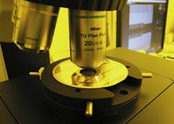
With the ConfoSurf CLV150, Lumics is now able to measure microstructures; in particular, structural dimensions, surface properties, and thicknesses. The optical measurement system is particularly useful in the optimization of the coating process since transparent coatings are needed in Lumics processes. Confovis can measure reflective materials and transparent coatings, allowing analysis of coating thickness and quality of the coating sidewalls with little effort and in a non-destructive manner.
With a vertical resolution of less than 3 nm, in accordance with VDI 2655, the CLV150 can also measure roughness in accordance with DIN EN ISO 4287/4288 or in accordance with DIN EN ISO 13565 or on the basis of surfaces in accordance with DIN EN ISO 25178.
"This [Confovis], especially, is what allows us to determine the depth during the etching process very precisely without stripping the coating from the wafer completely before measurement and re-coating it again after the measurement," says Kaebe. The parameters measured are compared with the calculated target values. These are heavily dependent on the epitaxy of the substrates and must to some extent be adjusted very individually. It is therefore useful to measure the etching depths or coating thicknesses again precisely between the process steps with the CLV150.
The measurement data recorded with the ConfoVIZ measurement software is subsequently transferred into the MountainsMapanalysis software. There, among other things, the companies say it is possible to quickly and simply set up and create protocols for error analysis. Lumics says that with the Confovis system that they have been able to continuously increase process yields.
SOURCE: Confovis; http://www.confovis.com/company/news/newsdetail/article/messtechnik-fuer-schnelle-prozessueberwachung-in-der-diodenherstellung.html
About the Author

Gail Overton
Senior Editor (2004-2020)
Gail has more than 30 years of engineering, marketing, product management, and editorial experience in the photonics and optical communications industry. Before joining the staff at Laser Focus World in 2004, she held many product management and product marketing roles in the fiber-optics industry, most notably at Hughes (El Segundo, CA), GTE Labs (Waltham, MA), Corning (Corning, NY), Photon Kinetics (Beaverton, OR), and Newport Corporation (Irvine, CA). During her marketing career, Gail published articles in WDM Solutions and Sensors magazine and traveled internationally to conduct product and sales training. Gail received her BS degree in physics, with an emphasis in optics, from San Diego State University in San Diego, CA in May 1986.