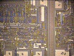
Terahertz wafer scanner from ARP detects chip defects down to 1 nm
Harrisburg, PA--A terahertz wafer scanner from Applied Research & Photonics (ARP) detects chip defects down to 1 nm, decreasing rejects in wafer fabrication. ARP says that chip manufacturers face a daunting challenge of keeping the “rejects” down in the wafer fabrication process. While a blank wafer costs only a few hundred dollars, a processed wafer can be worth hundreds of thousands of dollars depending on the end product, tremendously increasing costs if the wafer is rejected towards the end of the fabrication process. To reduce wafer fab rejects, ARP has introduced a non-destructive sub-surface scanner with a resolution of 1 nm by using its continuous-wave (CW) terahertz technology.
In the inspection stage, a wafer is rejected when the accumulated number of defects on a wafer exceeds the prescribed limit. Unfortunately, ARP says the current state-of-the-art (SOTA) high-cost and high-sensitivity inspection machines available in the marketplace fail to detect defects that are hidden below layers. Consequently, a wafer may pass the inspection process, but the final device will fail because the inspection system was not able to detect the smaller and hidden defects. For example, says ARP, a SOTA inspection system that costs on the order of a million dollars has a resolution of 0.15 µm (150 nm) and will miss defects smaller than this size. As the modern fab process is defining feature sizes down to 60 nm or less, the fab inspection technicians are faced with the challenge of detecting and identifying defects that are only a few nanometers in diameter. ARP says it addresses this deficiency by introducing a terahertz scanner with a resolution of 1 nm.
Modern fab processes involve layer-by-layer construction and defining devices on a wafer (the so called bottom-up process) where tens of layers are stacked one on top of the previous. Common optical inspection system can see only on the surface and the resolution is limited. Thus, defects buried under the top surface must be detected early in the process before it progresses towards completion. This is not possible by instruments built around visible light or IR which is offered by the current SOTA.
Terahertz can penetrate most materials except metals; thus, it provides the opportunity to inspect not only the surface but also the sub-surface interior layers of a multi-layered substrate. Unlike X-ray, terahertz is non-ionizing; therefore, it does not perturb or damage delicate features which in some cases are only a few nanometers in size. The combination of terahertz properties and a smart positioning system incorporated in ARP’s terahertz inspection provides unique opportunity to successfully inspect wafers at early stage of defect formation as well as after-process device failure analysis.
ARP is a dendrimer nanotechnology company with the core products in the terahertz area. ARP’s terahertz spectrometer, TeraSpectra (www.arphotonics.net), uses a high-power terahertz source enabling high-res resolution spectrometry in a 30 THz window for probing molecular phenomena on time scales from a few femtoseconds to a few tens of picoseconds.
SOURCE: ARP; http://terascanr.blogspot.com/2012/11/arp-deploys-terahertz-sub-surface.html
About the Author

Gail Overton
Senior Editor (2004-2020)
Gail has more than 30 years of engineering, marketing, product management, and editorial experience in the photonics and optical communications industry. Before joining the staff at Laser Focus World in 2004, she held many product management and product marketing roles in the fiber-optics industry, most notably at Hughes (El Segundo, CA), GTE Labs (Waltham, MA), Corning (Corning, NY), Photon Kinetics (Beaverton, OR), and Newport Corporation (Irvine, CA). During her marketing career, Gail published articles in WDM Solutions and Sensors magazine and traveled internationally to conduct product and sales training. Gail received her BS degree in physics, with an emphasis in optics, from San Diego State University in San Diego, CA in May 1986.
