Test and Measurement: Surface-measurement stitching technique scales to all sizes of optics
Paul Pulaski, Daniel R. Neal, and T. D. Raymond
A novel surface-measurement technique uses a reflective Shack-Hartmann wavefront sensor to scan optical surfaces and then uses software to stitch individual measurements together, resulting in high-resolution accuracy and high dynamic range with the ability to scale up or down to any size optic.
The competing requirements of accuracy, spatial resolution, dynamic range, and large field of view limit many optical measurement techniques. To address these limitations, WaveFront Sciences has developed a technique that scans and stitches together subaperture data to enable surface topology measurements with high resolution, accuracy, and dynamic range, along with a large field of view determined by the scan range. Using a Shack-Hartmann wavefront sensor that measures the reflective optical phase from a light beam incident on the surface, the optical phase can be directly related to the surface-height information that is mapped in two dimensions across the surface. After scanning the surface-either by a lateral scan of the reflective wavefront sensor system across the surface or by keeping the sensor fixed and laterally translating the surface relative to the sensor-individual measurements are stitched together by sophisticated software algorithms that scale over a range of dimensions from 100-mm wafers up to mirrors larger than 1 m in diameter.
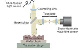
As an alternative to interferometric techniques for surface topology measurements, the Shack-Hartmann wavefront sensor does not require any vibration isolation and alignment is fairly straightforward. A metrology device to measure the nanotopography of silicon wafer surfaces uses this wavefront sensor to optically probe the wafer surface and nondestructively measure topography and site flatness with measurement sensitivity comparable to interferometric techniques (see Fig. 1).1 Unlike an interferometer, which requires a long settling time for the wafer, the Shack-Hartmann sensor measures the slope directly, permitting high-speed measurement via the stitching technique.
The Shack-Hartmann wavefront sensor
The basic elements of the Shack-Hartmann sensor are a microlens array, a mounting housing, and a megapixel digital CCD camera.2 The microlens array is produced on a fused-silica substrate using gray-scale photolithography and plasma etching.3 Each lenslet in the array has a 0.28-mm-square aperture and a focal length of approximately 28 mm. The square array is bonded to a metal fixture that constrains its position relative to the active area of the digital camera. Light incident on each lenslet of the array produces a focal spot on the CCD, where the local tilt of the phase front determines the position of the focal spot. By accurately determining the focal-spot positions in both directions, the wavefront “gradient” is deduced. The light incident on the CCD is digitized to 12 bits, pixel-by-pixel, and read into a personal computer, which then uses advanced centroid or convolution techniques to determine the focal-spot positions.
During sensor calibration, collimated light is reflected from an optical flat with flatness better than λ/20 and directed through the optical system to the sensor. A reference file containing the focal-spot positions is saved for later use. During normal operation, the light reflected from the wafer is also directed through the optical system to the sensor and the deviation of the spot locations in each direction provides the surface gradient of the wafer. Note that acquiring the reference file through the actual optical system automatically corrects for imperfections in the optical system.
Stitching measurements
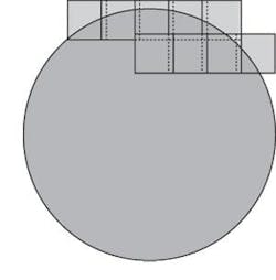
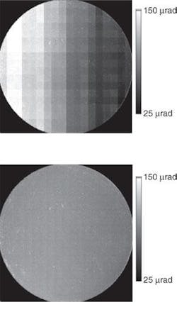
The data-acquisition method described previously permits the measurement of the wafer surface gradient over only a 14‑mm2 region of the reflective surface. To map a large-aperture surface, the translation stage is used to position the object (in this case, a wafer) to successively different locations; the laser is pulsed at each location and the surface gradient is recorded for the corresponding 14-mm2 frame. Unfortunately, the average tilt of each frame is affected by the imperfections in the stage bearings. To overcome this limitation, the stage is programmed to permit the measured regions to overlap by a few millimeters (see Fig. 2). The slope measurements in the overlap regions are used in a linear least-squares fitting routine to determine the relative tilts between frames of data. These relative tilts are then used to correct the data and to construct a stitched gradient map for the wafer (see Fig. 3).
The mechanical stage can introduce more than 100 µrad of tilt that is easily corrected by the fitting routine. This technique is routinely applied to aspheric surfaces of 300-mm aperture with sag as large as 200 µm and maximum tilt angles approaching 1.5 mrad without the need for goniometric stages.
An important requirement for this stitching technique is that the overlap region must be imaged twice to yield two distinct averages. If there were no change in net tilt between frames, these averages would yield the same value. In practice, each frame has a net tilt that is part of the average and the net tilts are different. The main task becomes finding a set of frame tilts that minimizes the differences between averages in the overlap regions.
The stitching algorithm needs to be general enough to cover arbitrarily shaped surfaces such as the circular wafers that yield a nonrectangular quilt pattern. A mathematical function accounts for frames of data that lie on an edge or corner of the surface and determines whether data exists within the frame. After the grid is established, then a merit function is generated that yields a system of equations by setting the derivative of this merit function to zero. These equations can then be cast into a data matrix form that is solved to minimize the difference in tilts. Because only relative tilts are being measured, the absolute tilt of the quilt cannot be determined, which is similar to electrostatics in which one solves for potential differences, not the absolute potential. The point is that one may wish to add a constant to the tilts such that the median tilt is zero, or one can choose a single frame to be the fiducial and force the tilt within that frame to zero and adjust all other panels accordingly.
Once the map of the surface gradient is obtained, the entire surface itself is reconstructed using a wavefront reconstructor algorithm. For these data one can use a successive (or simultaneous) over-relaxation method to numerically solve for the reconstructed surface.
Extension to other applications
Depending on the design of the reflective optical system, this stitching technique can be extended to any large or small optical surface. If the goal is to scan across a smaller optical surface with finer resolution, then the relay-imaging telescope that is part of the reflective optical system would simply be adjusted to achieve the desired resolution by incorporating an appropriate microscope objective. In this case the images taken by the wavefront sensor could be stitched together to achieve a high-resolution map of the surface.
Conversely, if the optical surface under test is too large to be placed on a translation stage, then the sensor can be translated laterally to scan across the surface. One example of this is measuring the surface topology of a very large mirror where a gantry system is used to scan the sensor. The reflective optical system including a light source is either connected to the translated sensor or the incident light source. In this case, the average tilts introduced by the mechanical system that is translating the wavefront sensor system would need to be corrected using a similar stitching algorithm described above. This method is suitable to measure large mirror segments for large-scale telescope projects. ❏
REFERENCES
1. T. D. Raymond et al., Proc. SPIE 4809, 208 (2002).
2. R. B. Shack and B. C. Platt, JOSA 61, 656 (1971).
3. P. Pulaski et al., Proc. SPIE 4767, 44 (2002).
PAUL PULASKI is optical engineer, DANIEL R. NEAL is technical director, and T. D. RAYMOND is research scientist at WaveFrontSciences, 14810 Central Ave. SE, Albuquerque, NM 87123-3932; e-mail: [email protected].


