Position-sensitive Detectors: Graphene/silicon position-sensitive detector has enhanced sensitivity, IR capability
The position-sensitive detector (PSD), which senses the position of a spot of light on its surface (whether the spot is stationary or moving), is a very useful optical detection and measurement tool for not just the optics laboratory, but for various types of instruments and optical systems as well. The PSD consists of an undivided silicon (Si) photosensing device that measures spot position through peripheral electrodes via the lateral photoeffect (this is in contrast to the so-called quad cell—a Si detector that has a similar function, but which has four separate quadrants and where spot position is measured by calculating the ratio of quadrant outputs).
However, the conventional PSD has limits in sensitivity that prevent the position measurement of spots of light with powers less than the microwatt level. As a result, laser systems—for example, laser guiding systems—that determine physical variables such as position, distance, displacement, and angle via spot-position measurement on a PSD are limited in range and other desirable characteristics.
In addition, conventional silicon PSDs operate in the visible region. If a PSD is needed for infrared (IR) use, one must be used that is based on thermopile detectors, which have slow response and require a cooling system.
Researchers from Southeast University (Nanjing, China) and the Suzhou Institute of Nanotech and Nanobionics at the Chinese Academy of Science (Suzhou, China) have found a way around the sensitivity limits for silicon PSDs by incorporating graphene into the Si, resulting in a graphene-Si heterostructure. As a bonus, the graphene-augmented PSD can operate in the near-IR out to telecommunications wavelengths (1319 and 1550 nm).
Pinning effect
The experimental PSD consists of a monolayer of chemical-vapor-deposition (CVD)-grown graphene placed on an n-doped Si substrate—four nickel-gold electrode strips in a square shape atop the graphene collect the signal. The back of the Si is coated with aluminum to serve as a common ground electrode. The prototype has an 8 × 8 mm operating area.
When the graphene is in contact with the Si, a “pinning effect” because of the surface states produce a band bending at the Si surface depletion layer, producing a built-in electric field. When light hits the device, electron-hole pairs produced in the Si surface depletion layer become separated by the built-in electric field, with electrons sweeping into the bulk Si and holes amassing at the surface, producing a lateral voltage gradient between illuminated and unilluminated areas. The diffusion length is enlarged greatly by the fact that the Si and graphene form a Schottky junction at the interface. Because graphene absorbs light and produces photogenerated carriers, the operating wavelength of the PSD is extended because of broadband absorption.
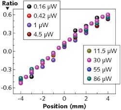
The device was tested with a spot of laser light at varying intensities and a wavelength of 532 nm, and spot size was also varied from 5 to 800 μW. The detector’s position-sensing performance at spot powers from 55 μW down to the nanowatt level (160 nW) agree well with each other (see figure). As with conventional PSDs, the position of the spot depended only on the “center of gravity” of the spot and not the spot size.
Using an acousto-optic modulator, the transient performance of the PSD was tested at a 633 nm wavelength. The device showed exponential rise and fall times of 430 and 450 ns, respectively, with the spot located near an electrode, and up to about 5 μs at the center of the PSD. This dependence of rise time on spot position is likely because of a longer transit time for holes produced farther from an electrode.
Finally, sensitivity to near-IR light was tested at 1319 and 1550 nm, showing linear and power-independent operation. The minimum operating power at 1319 nm was about 10 μW and 1550 nm was at the milliwatt level.
REFERENCE
1. W. Wang et al., Optica (2018); https://doi.org/10.1364/optica.5.000027.
About the Author
John Wallace
Senior Technical Editor (1998-2022)
John Wallace was with Laser Focus World for nearly 25 years, retiring in late June 2022. He obtained a bachelor's degree in mechanical engineering and physics at Rutgers University and a master's in optical engineering at the University of Rochester. Before becoming an editor, John worked as an engineer at RCA, Exxon, Eastman Kodak, and GCA Corporation.

