Industry turns to Raman spectroscopy as tool
Industry turns to Raman spectroscopy as tool
Harry Owen and Michael Pelletier
Compact solid-state lasers, improved CCDs, and novel optics enable practical Raman instruments expected to generate growth for applied spectroscopy in process measurements.
Athough the discipline of applied spectroscopy has been recognized for more than 50 years, its potential remains unfulfilled in many industries such as petrochemicals, polymers, pharmaceuticals, foodstuffs, cosmetics, and even the relatively high-technology field of semiconductor manufacturing. All these industries rely on various types of instruments to make compositional measurements for monitoring processes such as fermentation, distillation, or mixing. Most of these process analyzers do not use spectroscopy, but rather are based on chemical-separation techniques such as chromatography. For example, various estimates indicate that gas chromatographs alone account for around 30% of the $1 billion market for process analyzers.
The major advantage of optical spectroscopy over other techniques is its capabilities for real-time measurements. For example, a high-performance liquid-chromatography (HPLC) analysis of a biochemical fermentation mixture may take only a few minutes, but the typical sample preparation for HPLC could easily add an hour to this time. Similarly, the conventional octane measurement test requires that one pint of gasoline be burned in a reference engine over a 20-minute period. However, a modern Fourier-transform infrared (FT-IR) or Raman spectrometer can acquire a complete diagnostic spectrum in seconds or less, giving virtually instantaneous quantitative data.
Additionally, "chemical" techniques require removal of a test sample to a laboratory setting where the instrument is housed. Spectroscopy offers the potential of direct in situ testing of processes, particularly with the use of low-cost fiberoptic sampling accessories. This, in turn, permits closed-loop process control.
Overview of spectroscopic techniques
Given these factors, why doesn`t spectroscopy have a larger share of the important process instrumentation market? One simple answer is that, until recently, the major optical techniques (FT-IR, near-IR, and Raman spectroscopy) have all had significant limitations and drawbacks for direct process analysis and control. For example, FT-IR spectroscopy is a popular and powerful tool for laboratory chemists, particularly for analyzing organic materials. Typical IR absorption spectra consist of sharp peaks and bands that can be easily assigned to characteristic molecular frequencies. Peak height (versus baseline) can be calibrated to give accurate absolute species concentrations.
Unfortunately, FT-IR spectroscopy is difficult to implement for real-time process analysis because of sampling problems. Mid-IR transmission measurements usually require very short path lengths (10 µm or less), and often Beer`s law is violated because of high absorbances. Alternatively, the IR radiation may be coupled directly into the sample using attenuated-total-reflection (ATR) devices. These can introduce interface artifacts due to sample film build-up.
For process analysis, near-IR (NIR) absorption spectroscopy is easier to implement. Near-IR wavelengths (1-2 µm) transmit well through low-cost glass fibers, and water absorption is not too problematic. In addition, modern solid-state spectrometers have no moving parts, maintaining calibration even in hostile environments. However, the major drawback is that the absorption features in this spectral region correspond to high-order overtone vibrations of molecules. Because any chemical species has many combinations of these overtones, even a pure sample spectrum consists of a number of overlapped broad features, with few sharp resonances and no true baseline.
As a result, direct analysis of NIR spectra of real samples may be impossible. Rather, the instrument`s software must be empirically trained with a large number (often more than 100) of reference samples to correlate overall spectral characteristics with composition. This approach--chemometrics--is fraught with inherent limitations. Any change in a process requires the preparation of new samples and the complete revalidation of the chemometrics method being used. In many industries, formulation changes or changes in raw materials are frequent, making total reliance on this approach undesirable.
Raman spectroscopy combines the favorable aspects of both these other techniques, but until recently the technique has suffered from serious instrumentation limitations. The development of several new technologies has eliminated these limitations.
Like FT-IR spectroscopy, Raman spectroscopy detects fundamental molecular vibrations, producing clean, sharp peaks that can often be unequivocally assigned to chemical species. But both the excitation laser and the Raman-scattered light are in the visible or near-IR regions and thus can be transmitted through conventional glass fiberoptic devices. Furthermore, Raman spectroscopy produces only a weak water signal so that the components of aqueous samples can be readily detected and analyzed. What`s more, no part of the Raman system ever needs to touch the sample; semi-confocal operation can even eliminate a signal from a window-sample interface, reducing the importance of film build-up.
However, chemical technicians and engineers want push-button simplicity, and, until recently, Raman instrumentation could not be delivered in this form. Raman scattering is a low-probability event that benefits from laser excitation. For an incident light level of 1, typical Raman signals are in the 10-8 range. In the past, Raman spectroscopy has been performed using a single-frequency gas laser--often a bulky argon-ion laser at 488 or 514 nm. To eliminate laser scatter, the Raman signal was then filtered through a double or triple scanning monochromator, with typical losses of about 95%. Such systems were very cumbersome, often covering an entire optical table. More important, they required expert maintenance and frequent realignment, making them unsuitable for industrial process analysis and therefore only rarely used for routine laboratory work.
Recent advances in Raman technology
Fortunately, three critical enabling technologies have changed this situation: high-efficiency holographic filters and elements; compact, high-power solid-state lasers; and low-noise charge-coupled-device (CCD) detectors. This combination has resulted in a Raman instrument that delivers the key practical features demanded by the process-control market: ruggedness, compact size, and operation by semi-skilled individuals (see Fig. 1).
The source is a compact solid-state laser, either a frequency-doubled, diode-pumped Nd:YAG laser at 532 nm or an actively stabilized diode laser (typically at 785 nm). Both laser types require very little maintenance, with typical lifetimes of many thousands of hours. The green source is often favored by users who were previously familiar with argon-ion-laser Raman excitation. However, many researchers prefer the NIR laser, which results in fewer problems from sample fluorescence, particularly for agricultural products, foodstuffs, and cosmetics.
A critical component of this Raman instrument is the holographic notch filter used to eliminate Rayleigh-scattered laser light. This SuperNotch-Plus filter combines high extinction (10-6) with high efficiency and narrow bandwidth, enabling detection of low-frequency Raman signals, for example, shifted only 50 cm-1 from the laser line. The filter thus eliminates the need for a triple monochromator for most applications.
In the HoloProbe family of Raman spectrometers from Kaiser Optical Systems (Ann Arbor, MI), the prefiltered Raman scatter is then dispersed using a second holographic optical element--a transmission diffraction grating. The dispersed light is imaged onto a cooled CCD array, interfaced to the spectrometer`s dedicated PC. Using an array detector to replace slit scanning is key to fast data acquisition. In addition, the CCD allows multiple spectra to be simultaneously recorded using several fiber probes. The novel HoloPlex grating also avoids the usual trade-off of resolution versus spectral coverage by acting as two gratings; it separately disperses the long- and short-wavelength portions of the spectrum, imaging them at different heights on the CCD detector.
Flexibility adds to the utility, and, hence, value, of this type of instrument. For example, Kaiser offers a universal probe interface (with holographic optics) that allows the same instrument to be interfaced to an optical microscope for identification of minute particulates and samples, to hundreds of meters of fiber for remote sensing, to a telescopic probe for remote short-range monitoring, and to a standard cuvette setup.
Wet semiconductor processing
For some applications in the pharmaceutical and petrochemical industries, Raman spectroscopy often simply replaces inferior test methods. But, in other applications, Raman spectroscopy has the potential to enable tests and checks that were previously intractable or not cost-effective. An excellent example in this latter category is in the early stages of investigation in the field of semiconductor fabrication.
Sematech (Austin, TX) is a government/industrial consortium performing research in the semiconductor area. Ronald Carpio is a research scientist at Sematech currently investigating ways to more tightly control some of the wet-chemical processes. He explains, "Modern semiconductor fabrication demands increasingly tight control of wet chemistry such as wafer etching and cleaning. However, although these processes have been around for at least 25 years, no simple (push-button), reliable method has yet been developed to monitor critical-solution concentrations."
Recently, Carpio and engineers at Kaiser Optical Systems (Ann Arbor, MI) have collaborated in an investigative study of Raman spectroscopy for this application.1 The main focus of this study was SC-1, a cleaning solution used to remove contaminants from silicon wafer surfaces. SC-1 is an aqueous mixture of hydrogen peroxide (H2O2) and ammonium hydroxide (NH4OH). When the ammonia/peroxide ratio is too high, etching produces a rough surface that can lead to degraded oxide gate breakdown.2 Conversely, when this ratio is too low, the result is inefficient particle removal.3
Water and ammonia are volatile, and hydrogen peroxide is unstable. Because the cleaning process involves elevated temperatures (60°C-80°C) and recirculation agitation, the composition of SC-1 thus varies with use and time. Until recently, this necessitated frequent replacement of the ultrapure SC-1, which is expensive to purchase and dispose of. Replacement also results in unnecessary downtime to bring the cleaning baths back up to temperature. To reduce these problems, the approach of spiking the SC-1 baths with fresh chemicals is adopted in some facilities, but this creates concentration compositions that can be quite inaccurate.
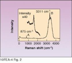
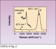
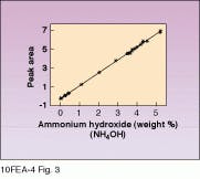
Figure 2 shows a typical Raman spectrum of an SC-1 sample obtained with a HoloProbe Raman instrument equipped with a 50-mW, 532-nm frequency-doubled Nd:YAG laser. The peak at 875 cm-1 marked A is due to hydrogen peroxide. The sharp feature marked B at 3311 cm-1 is an ammonium hydroxide (NH4OH) band. The broad underlying band is due to water. The A and B peak areas were found to correlate very well with species concentration, giving R values of 0.9993 for NH4OH (see Fig. 3) and 0.995 for H2O2. Furthermore, the data indicate that the R correlation value for H2O2 could be raised even higher by allowing for the slight dependence of H2O2 peak height on the NH4OH concentration.
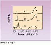
Prompted by these very promising results, researchers also studied Raman spectra of other wet-chemical solutions common to the semiconductor industry (see Fig. 4). Many people imagine that precision process control is a hallmark of semiconductor processing, so the inability to accurately measure these rather fundamental factors probably comes as a surprise. While we wish to stress the preliminary nature of these Raman results, they do indicate that Raman spectroscopy could be the real-time technique to finally deal with the increasingly important problem of wet-chemical concentration monitoring.
Using the latest in electro-optics technology, it is now possible to build a Raman spectrometer that has rugged solid-state construction and no moving parts. These instruments fit in a sealed box no bigger than a desktop computer and include powerful system software allowing push-button acquisition and processing. With the inherent benefits of Raman measurements compared to other spectroscopic techniques, this Raman instrument should facilitate the application of the technique in a wide variety of industrial process-control environments. n
ACKNOWLEDGMENT
The authors wish to acknowledge the invaluable assistance of Dr. Ronald A.Carpio of Sematech (Austin, TX).
REFERENCES
1. M. J. Pelletier, K. L. Davis and R. A. Carpio, Proceedings Symposium on Process Control, Diagnostics and Modeling in Semiconductor Manufacturing I, Electrochemical Society, Reno, NV (May 1995).
2. M. Meuris et al., Jpn. J. Appl. Phys. 31, Part 2, L1514 (1992).
3. M. Itano, F. W.Kern, Jr., M. Miyashita, and T. Ohmi, IEEE Trans. Semicond.Manufact. 6, 258 (1993).
FIGURE 2. SC-1 cleaning solution used in semiconductor industry has characteristic peaks that can be monitored with Raman spectroscopy. Peak A is H2O2, B is NH4OH. Inset expands peak A.
FIGURE 3. Calibration curves must be determined before Raman spectroscopy can be used in process environment. For NH4OH, based on peak B in Fig. 2, the correlation is excellent (R = 0.9993).
FIGURE 4. Different cleaning solutions have characteristic peaks, therefore Raman spectroscopy can be used to identify other cleaning solutions for the semiconductor industry. A is HCl/H2O2/water; B is H3PO4/H2O2/water, and C is H2SO4/H2O2/water.
HARRY OWEN is director, laser spectroscopy products, and MICHAEL PELLETIER is senior scientist at Kaiser Optical Systems, 371 Parkland Plaza Rd., Ann Arbor, MI. 48103.


