Modularity redefines the atomic force microscope
by F. Michael Serry
The atomic force microscope measures a surface in three dimensions down to sub-Angstrom height variations, and characterizes the surface far beyond its topography. A modular AFM enables multiple applications in one instrument.
Soon after its invention in 1986, the atomic force microscope (AFM) established itself as a groundbreaking laboratory instrument that offered intriguing insights into the structure of solid matter. Since then, the AFM has evolved into an instrument with seemingly endless ways of probing and revealing the secrets of a sample's surface. Commercial AFMs are powerful and flexible modular instruments by many definitions.
A basic description of how the AFM works provides insight into the prevalence and importance of modularity in the instrument. The AFM raster scans the surface of a sample, in air or in a liquid, with a sharp tip (5- to 30-nm end radius), integrated in a microfabricated cantilever beam of silicon or silicon nitride. By detecting and controlling one or more (in a long list) of short- and long-range tip-sample interactions, the AFM extracts information about the surface, and presents it in the form of one or more three-dimensional images. Because a large range of functionality is inherent in the operation of a typical AFM, modularity in the equipment, techniques, and software has evolved primarily to realize the instrument's potential and flexibility.
In the most prolific atomic-force microscopy imaging modetapping modethe tip makes intermittent (typically 300 kHz) gentle contact with the sample. In the second most popular modecontact modethe tip is in perpetual contact with the sample. Imaging the topography in these two modes powers the largest number of applications by allowing three-dimensional visualization, individual feature measurements, and statistical measurements such as surface roughness. Tapping mode and contact mode also allow numerous derivative modes of surface characterization, giving rise to additional images beyond topography that reveal to the researcher the electrical, magnetic, mechanical, chemical, and other properties of the sample.
Tip modularity
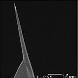
An important factor underlying the modularity of the AFM is the explosion in the variety of probes, also called tips. Hundreds of different tip types are available from numerous manufacturers around the world. While most tips are optimized to work well for many common applications, like topography imaging, some tips are so customized as to be useless for all but one or two specific applications, for which no other tips work (see Fig. 1).
To help the AFM user take advantage of the great variety of tips available, AFM manufacturers have made it easier and faster to change the tip. It often takes an experienced user less than a minute to exchange the tip, make the necessary alignments with the laser, detector, or other component, and continue operating the instrument. Some AFMs are so advanced that tip exchange is automated, requiring no operator intervention. Similarly, tip manufacturers have played their part by making their tips compatible with the majority of AFMs on the market. As a result of this market-driven symbiosis between tip and instrument manufacturers, the typical AFM user enjoys a measure of modularity that has few, if any, parallels in the analytical instrument market.
Technique modularity
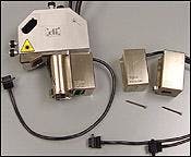
Another factor behind the modularity of the AFM is the variety of probing techniques the instrument supports. These techniques are made possible in two ways. One is by changing a part on the AFM. For example, by changing the sensor the AFM can switch from one mode of operation to another (see Fig. 2). A second level of modularity enables the user to select different operating techniques via software rather than change hardware.
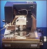
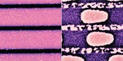
For example, in a software-controlled dual-mode operation an AFM can capture a contact-mode topography image and a (contact-mode derivative) scanning capacitance microscopy (SCM) image simultaneously using all the same hardware, including the same tip (see Fig. 3). The SCM image is a map of the density of electric-charge carriers (usually of interest in electrical or electro-optical devices). The (contact-mode derivative) scanning thermal microscope (SThM) image, a map of temperature variation, requires changes in the AFM hardwarereplacing the SCM sensor with an SThM sensor, and the SCM tip with a highly specialized thermal tip. Image combinations like those in Fig. 3 have established an impressive track record of discovery, particularly in failure analysis of semiconductor lasers and optical detectors.
With the right tip and choice of software parameters, a user can investigate electrical, magnetic, chemical, adhesion, elasticity, and a myriad of other properties about a sample. In another example, a simultaneous scan using all the same hardware (including a magnetically coated AFM tip), simultaneously provides a tapping mode topography image and a tapping mode-derivative magnetic- force-microscopy (MFM) image that reveal the structure of tracks and magnetic domains of the bits on a magneto-optical storage disk (see Fig. 4).
Data modularity
The AFM image itself is modular in that once the AFM captures an image, a wealth of techniques is available for visualizing and quantitatively analyzing the data. A single three-dimensional AFM image allows visualization from endless viewing angles at adjustable aspect ratios and zooms. This is an advantage over the two-dimensional image (micrograph) provided by scanning electron microscopes (SEMs). Each AFM image is the equivalent of numerous SEM micrographs, which often require repositioning of the sample and detector and adjusting the electron beam.
An AFM image can reveal height, length, width, and angle of individual features, such as a defect in a microelectromechanical system (MEMS) micromirror or a line on a photolithography mask. It can also reveal statistical information, such as the roughness of a mirror, the periodicity (pitch) of a grating, the spectrum of the surface topography of, for example, a quartz substrate or a thin-film coating.2 Indeed, AFM statistical data analysis has proven particularly successful for controlling low-scatter optical thin films.3 Many AFM manufacturers have loaded their software with image manipulation and analysis options to take advantage of the modularity of data.
One of the most useful options is the ability to juxtapose two or more images for correlation, and extracting information that is clearly visible only when the images are combined. An excellent example of this was first published in 1998.4 The topography image and SCM images of a gallium nitride (GaN) film grown on sapphire appeared side-by-side, as well as combinedone image first inverted (image inversion being a useful feature in itself) and then superimposed on the other. The combined image revealed that threading dislocations, commonly found on such samples, had a strong effect on the distribution of dopant atoms along the area under study.
Commercial AFM-instrument and tip manufacturers provide a variety of options that add to the modularity of the AFM. Glass cells allow imaging in liquid, sample heaters make possible investigating materials at elevated temperatures, and electrochemical attachments and software enable the study of corrosion. As the scientific community continues to use the AFM, new applications will drive the invention of techniques and options, and expand the modularity of the AFM.
REFERENCES
1. See www.di.com/appnotes/SCM/SCMHLaser.html.
2. Micromachine Devices 7(2), Cahners Publishing (March 2002).
3. See www.di.com/AppNotes/ThinFilms/TFmain.html#SRC4.
4. Appl. Phys. Lett. 72(18) 2247 (May 4, 1998).
F. MICHAEL SERRY is an applications scientist at Digital Instruments/Veeco Metrology Group, 112 Robin Hill Rd., Santa Barbara, CA 93117; e-mail: [email protected].


