Lenslet arrays measure aberrations in like devices
In recent years, the demand for various types of microlenses has grown in applications ranging from light coupling in optical communication systems to lenslet arrays in wavefront sensors. With this increase in applications, precision testing of microlens quality has grown as well. The most common technique to measure wavefront aberrations in optical systems involves an interferometer, which requires vibration-isolation platforms, reference optics, and tedious alignment procedures.
The use of a Shack-Hartmann wavefront sensor is an alternative to interferometric techniques that eliminates the need for vibration isolation and complicated alignment.1, 2, 3 Such a wavefront sensor consists of a specially mounted micro-optic lenslet array in front of a CCD array. The wavefront sensor measures the wavefront characteristics of a light beam that is either transmitted through an optical element or reflected off of an optical surface such as a lens or mirror.
Individual lenslets sample the light and create a series of focal spots onto the finely spaced CCD array. These focal spot positions are measured and the centers of the spots (known as the centroids) are calculated by determining their center-of-mass coordinates. The centroid positions from the focal spots of the test beam are compared with the centroid positions from a carefully constructed reference file. This reference file allows for the minimization of effects from imperfections in the CCD array, lenslet arrays, and imaging system.
From this data, the average gradient of the wavefront over each lenslet can be calculated from the difference between the centroid positions and those of the reference wavefront, which can be integrated to provide the reconstructed wavefront of the incident radiation using both local (zonal) and global (modal) methods. The output from the modal method can be a set of Zernike polynomials that relate to the aberrations present in the wavefront.4 The zonal method derives a set of relations for the phase given a number of slope measurements.5
Micro-optics fabrication
Several techniques are used to fabricate micro-optics, including molding technology, ink-jet printing technology, and photolithography. We use photolithography to fabricate micro-optics. This process includes designing a gray-scale mask to photolithographically pattern a photoresist-coated substrate (either fused silica or silicon) and then fabricating the microlenses or diffractive optical elements. The gray-scale mask has a high-resolution pattern with a range of optical densities (OD) used in the photolithographic process to pattern the photoresist. This pattern is then etched into the substrate using a plasma-etch process.
Normally, each microlens has at least 32 levels designed to approximate the contour of the surface of the lens. The gray-scale process, however, can yield up to 500 levels. This photolithographic technique can manufacture a lenslet of any shape. Our standard lenslet arrays are made up of square lenslets with a 100% fill factor. In addition to the fabrication of the microlenses, the quality of the transmitted and reflected wavefronts is important.
Wavefront aberrations
The setup for the transmission and reflection measurements includes a single-mode fiber coupled to a 635-nm diode laser, an aperture converter, and our wavefront sensor. To avoid confusion, we note that there are two types of lenslet arrays in this setup—one is part of the wavefront sensor and the other is the lenslet array to be tested. There is a tradeoff between the sensitivity and the dynamic range of the sensor when choosing the focal length of the sensor lenslet array. Given the flatness of the test wavefronts, the focal length of the lenslet array inside the wavefront sensor is chosen to yield the highest sensitivity (since the dynamic range is small for these wavefronts).
The first step in making wavefront measurements with the Shack-Hartmann sensor is to create a reference file of a precisely collimated beam using a high-quality lens with a wavefront error of less than l/100 over the center 1-mm2 area of the lens. All the subsequent measurements are taken with respect to this reference file. The wavefront slopes at each lenslet are calculated from the difference between the measured and the referenced centroid positions.
To measure the transmitted wavefronts of fused-silica lenslets, we placed a fiber-laser source at a focal distance behind the test lenslet array (see Fig. 1). By masking off the largest circle enclosing the wavefront from an individual lenslet, and adjusting the position of the lenslet relative to the fiber point source, we ensured a "collimated" output beam incident on the wavefront sensor. The reflection measurements were taken with a collimated light source incident on the surface of the silicon lenslet arrays. The reflected wavefront then passes through the aperture converter and onto the wavefront sensor.
We took a random sampling of 20 individual lenslets from each of the test fused-silica and silicon lenslet arrays (with different focal lengths and diameters). Depending on the size of the individual lenslets, aperture converters were designed to expand the beam so that the image from a single lenslet filled a significant portion of the CCD sensor area. For each position of an individual lenslet, the wavefront measurement was averaged over 100 frames to reduce the effects of air turbulence. Both circular and square software masks were used to reconstruct the wavefront via modal and zonal methods, respectively.
By analyzing the Zernike decomposition of the wavefront from these lenslets with our modal method, we found that the Seidel aberrations such as astigmatism, coma, and spherical aberration do not play a significant role in the transmitted and reflected wavefront from these lenslets. The focus term from the reflected measurements allowed us to calculate the radius of curvature R, and subsequently the focal length of the silicon lenslets. Because the lenslet contours are spherical, the focal length is simply R/(n-1), where n is the index of refraction of silicon.
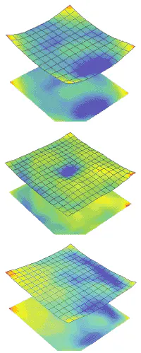
FIGURE 2. A zonal wavefront phase map represents individual fused-silica lenslets. The OPD and rms values are averaged over a random selection of 20 lenslets from each test array. Focal length = 8.2 mm, diameter = 0.144 mm, average P-V OPD = 0.229 waves, average rms wavefront error = 0.044 waves (top); focal length = 15.5 mm, diameter = 0.198 mm, average P-V OPD = 0.109 waves, average rms wavefront error = 0.016 waves (center); focal length = 25.1 mm, diameter = 0.252 mm, average P-V OPD = 0.137 waves, average rms wavefront error = 0.023 waves (bottom).
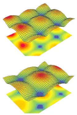
The zonal method was used to reconstruct the wavefront with a square mask encompassing the total area of an individual lenslet. The relevant parameters that were measured in this case are the P-V optical path difference (OPD) and the root-mean-square (rms) wavefront variation (or wavefront error). The OPD is the total peak-to-valley phase difference across the enclosed mask area and the rms variation is the root-mean-square of the reconstructed wavefront from the average OPD. Representative 3-D plots of the reconstructed wavefronts and the associated average OPD and rms wavefront error from each of the three sets of fused-silica lenslet arrays were obtained (see Fig. 2). The zonal wavefront from the two silicon lenslets arrays maps out the surface profile of the individual lenslets (see Fig. 3).
null
On average, the smallest diameter fused-silica lenslet yielded a significantly larger OPD and wavefront error. This is most likely because the f = 8.2-mm lenslet array has the smallest lateral feature sizes in the levels used to approximate the contour of the lenslets, compared to the other two test arrays. As this feature size decreases, the surface quality degrades slightly because of limitations in the fabrication process (near the corners of the lenslets), leading to more aberration of the transmitted wavefront. A slightly enhanced deformation of the zonal OPD occurs near the corners of all three test lenslets. This effect, however, is more pronounced for the smallest lenslet. Despite this enhanced OPD, the overall quality of the test lenslets is very good. The average P-V OPD for the transmitted wavefront through the fused-silica lenslets is less than l/4 and the average rms wavefront error is less than l/20.
PAUL D. PULASKI is an optical scientist at Wavefront Sciences, 14810 Central Av. SE, Albuquerque, NM 87123; e-mail: [email protected].
REFERENCES
- P. D. Pulaski et al., Proc. SPIE Ann. Meeting, 4767 (2002).
- D. R. Neal et al., SPIE, 2993 (1997).
- L. Erdmann et al., Appl. Opt. 37, 676 (1998).
- D. Malacara, Optical Shop Testing, John Wiley & Sons, New York, NY (1992).
- W. H. Southwell, JOSA 70, 8 (1980).


