Innovative laser design enhances micromachining applications
Innovative laser design enhances micromachining applications
Ed North
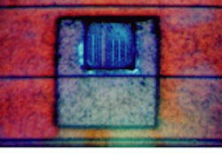
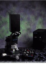
A small, flashlamp-pumped Nd:YAG laser manufactured by New Wave Research (Sunnyvale, CA) enhances semiconductor failure analysis and liquid crystal display (LCD) repair. Introduced in early 1996, QuikLaze is also an effective tool for resistor trimming and fuse blowing and can be used to cut metal buses, such as gold-on-ceramic multichi¥modules (see Fig. 1).
To perform repetitive tasks on successive devices, precision laser micromachining requires a work surface that can be moved in complex patterns and a means for viewing the processing area. To meet these needs, QuikLaze was designed so it can be fitted with a motorized stage that allows components to be moved in two dimensions under the beam. The beam can be focused using the optional Mitutoyo (Kanagawa, Japan) FS60 Series microscopes, as well as the A-Zoom from Ready Products (Irvine, CA).
Multiple wavelengths
The flashlamp-pumped laser operates at three wavelengths: 1064, 532, and 355 nm. To generate the second-harmonic output, designers used potassium titanyl phosphate (KTP), and to generate third-harmonic output, they used a crystal of beta-barium borate (BBO). The laser is internally cooled and Q-switched with a Pockels cell to generate pulsed output. The system produces 7-ns output pulses of u¥to 0.6 mJ of energy at pulse-repetition rates extending to 20 Hz.
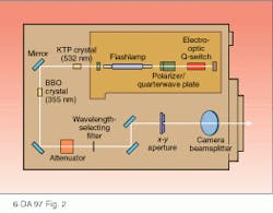
The three-wavelength design enables users to choose the appropriate wavelength for the materials being processed. A patented advanced beam delivery system changes wavelength selection with a switch. Operators can choose the optimum wavelength and energy during each ste¥of the micromachining process without having to change laser heads or manually insert dichroic mirrors and harmonic generators. A gear-driven filter wheel fitted with dichroic or absorbing filters mounted after the tripling crystal selects the wavelength of choice (see Fig. 2). The motorized, multiwavelength optical attenuator affords precise control of the laser energy at each wavelength.
The selected beam passes through a microscope objective, which focuses it down to a specified spot size. Special near-ultraviolet and near-infrared objective lenses allow coincident focus of visible and third-harmonic or visible and fundamental wavelengths, respectively. This allows the operator to view laser cuts as they are made, because the laser cutting beams are focused at approximately the same point as the visible light from the sample. A motorized x-y aperture enables users to select spot sizes ranging from 1 to 50 µm. Using the microscope`s 100X objective, QuikLaze can make cuts as small as 1 ¥ 1 µm, while a 50X objective permits cuts as large as 50 ¥ 50 µm.
Ambient light reflects off the sample and passes back through the microscope objective. Near the end of the beam delivery system, a 50:50 beamsplitter at 45° diverts some of the light reflected off the sample to a camera adaptor. The user can add a CCD camera to the system to view the target area and observe micromachining activity in real time on a video monitor.
Semiconductor machining
In semiconductor applications, QuikLaze generally is used as a supplemental tool to a focused ion beam (FIB) system. Currently, FIB systems have a distinct advantage over laser micromachining instruments in many semiconductor operations and therefore aren`t likely to be replaced by lasers anytime soon. In particular, FIBs are excellent micromachining tools for submicron geometries, although they are less effective than lasers in certain micron-level applications.
With a cost ranging from $500,000 to $1 million, however, FIB systems are expensive. By comparison, QuikLaze costs approximately $60,000 for the laser, depending on configuration. With a microscope, motorized stage, and other required accessories, the system typically can be purchased for less than $100,000.
In micron-level applications, QuikLaze operating at 355 nm is more effective than a FIB system at removing large areas of polyimide. This material is a relatively thick (approximately 3 to 5 µm) coating that serves primarily as a protective layer between the package and the semiconductor. When a semiconductor is defective or not working properly, polyimide must be removed prior to troubleshooting and repairing the device. After the material is removed, engineers take circuit measurements to determine which circuits are faulty. Once that is resolved, defective lines can be cut using either a laser or a FIB system. If further processing, such as adding new lines, is required, the ion beam is employed in a procedure called FIB editing.
At the 532-nm green wavelength, QuikLaze efficiently removes silicon dioxide from metal circuit lines and cuts them, an important task that helps IC design engineers improve productivity. The 1064-nm infrared wavelength also cuts metal circuit lines, with less likelihood of damage occurring to the silicon or gallium arsenide substrate.
QuikLaze has applications in LCD repair as well. The high repetition rate allows the system to remove shorts and defects u¥to 20 times faster than conventional 1-Hz, air-cooled lasers. As with other applications, the flexibility of multiple wavelengths is a crucial attribute. o
Figure 1. Nd:YAG laser for micromachining in semiconductor applications offers turnkey operation at three wavelengths through microscope objective. Inset shows polyimide and to¥metal layer removed from a semiconductor.
FIGURE 2. Output from Nd:YAG laser passes through KT¥crystal to produce 532-nm (second harmonic) output and BBO to produce 355-nm (third harmonic) output.


