Electrons probe to subangstrom levels
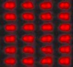
Images with a resolution of less than an angstrom were obtained from an electron microscope at Oak Ridge National Laboratory (Oak Ridge, TN).1 Steve Pennycook and other researchers incorporated advanced electron optics into a 300-kV Z-contrast (so-called because the return-electron intensity depends on the atomic number Z of the element being probed) scanning-transmission electron microscope (STEM), which allowed them to image silicon with a resolution of 0.6 Å (see figure).
The microscope will provide researchers with a valuable tool for designing advanced materials. The ability to image down to the level of single atoms provides an opportunity to understand the factors controlling optical (as well as electrical and mechanical) properties of nanostructures, interfaces, device junctions, and grain boundaries. “If we can see the atoms and how they get together,” explains Pennycook, “we can really see how materials work.”
The STEM is a hybrid between the more common scanning electron microscope (SEM), used for many types of optoelectronics research, and a transmission electron microscope (TEM). In optoelectronics research, TEMs are used less often than SEMs (which operate in reflection), because TEMs require that samples be only a few hundred atoms thick. This required thinning makes TEM a destructive tool. Nevertheless, TEMs provide higher resolution than SEMs and can see below the surface. They have been used to investigate the microstructures of nitride and phosphide (III-V) thin films, quantum dots and devices, photoluminescent silicon, and optical-recording media.
Scanning-transmission electron microscopes are still rather rare instruments because the possibility of forming useful direct images in this way has only developed in the last 15 years. Recently, with improving resolution, the technique of Z-contrast microscopy has gained popularity and it has been incorporated into commercial microscopes. About a hundred machines in the world exist with the potential to image at a 2-Å resolution, but of these fewer than 10 are aberration-corrected, and the Oak Ridge machine is the only one currently that can generate a subangstrom beam.
Scanned electron probe
Ordinary TEMs aim a planar wavefront of electrons at a thin sample, which scatters a number of the electrons. An objective lens after the sample forms a magnified image, from which the atomic structure can be deduced. In the STEM, in contrast, an electron lens before the sample focuses a beam of electrons to form a small probe, which is then scanned over the specimen. The scattered electrons seen by the annular detector build up an image as a function of the probe position. “The heavier the atoms are,” says Pennycook, “the more signal bounces off.”
The resolution of previous STEMs was limited by aberrations in the electron lenses. Several previous methods were used to obtain subangstrom images in spite of aberrations: by tilting the sample in comparison to the incoming beam of electrons in a TEM, the resolution in one axis could be increased, but information in the images becomes delocalized in the other direction. If the main lens is underfocused, it partially compensates for spherical aberrations and details in a narrow range of sizes can be seen. Unfortunately, detail at other sizes is lost.
The new method instead focuses on providing a smaller probe beam. In this way, no information is lost but finer details come into view. By correcting the aberrations in the electron lens, the aperture can be made larger, which in turn provides a smaller probe, resulting in better transverse resolution. The corrected lenses were provided by Nion (Kirkland, WA).
The larger aperture also results in a smaller depth of field, which leads to the possibility of using the microscope to image planes at different depths—effectively making an electron-microscope equivalent of a visual confocal microscope. Pennycook says the researchers are exploring this idea. “We want to look at all the new materials we can and in all the new ways we can,” he notes.
REFERENCE
1. P. D. Nellist et al., Science 305, 1741 (Sept. 17, 2004).
