Automated tests improve laser diode manufacturing
MARK KOENIG, RON HARTMAYER, PRABHU THIAGARAJAN, and ANDY QUINN
Increasing demand for fiber capacity has placed stringent performance requirements on the diode lasers used both for transmitting signals and pumping fiber amplifiers. Economic fabrication of these high-performance components in volume has in turn necessitated development of more fully automated production test equipment. At Spectracom (White Bear Lake, MN), a producer of 980-nm output diode lasers, automated test equipment is improving performance, increasing yields, and lowering cost of the final product.
Application requirements
The primary method for carrying multiple signals on a single optical fiber is wavelength-division multiplexing (WDM). The most-advanced systems (dense WDM or DWDM) now use 80 separate wavelength channels over a spectral range of 1532 to 1564 nm, with a channel spacing of only 0.4 nm. Erbium-doped fiber amplifiers (EDFAs) pumped by 980-nm output diode lasers amplify this signal for long-distance transmission.
One way to add more channels is to increase the EDFA gain, which requires increasing the output power of the EDFA pump laser. The challenge for manufacturers of these lasers then becomes producing higher-power devices with performance specifications that can be maintained over the entire lifetime of the system, even if it is subjected to extremes of temperature.
In the past, fiber-system integrators obtained 980-nm lasers by testing incoming devices and selecting those that met the criteria. Cost considerations are now driving these users to ask the laser manufacturers to take on this responsibility. In order to accomplish this economically, however, laser manufacturers must increase yields for in-specification lasers, rather than simply selecting lasers that meet specifications. This requires improved testing and process control instrumentation.
As a result, manufacturers have sought out instrumentation vendors that can combine diode laser control electronics, systems for measuring output and operating characteristics, and the requisite motion control into automated, turnkey diode laser test systems. Purchasing a total, vertically integrated testing solution is attractive to the laser makers because it eliminates the need for them to develop in-house expertise in disparate technologies, and it gives them a single vendor with sole responsibility for system operation.
Manufacturing process
Diode lasers are manufactured in a manner similar to other microelectronic devices. Starting with a substrate, the layer structure is built up with crystal growth techniques such as molecular beam epitaxy (MBE). The lasers are then made using photolithography and various chemical processes. A single 3-in. wafer typically yields as many as 7000 individual lasers. After the devices are fabricated, the wafer is scribed and cleaved into a number of bars, with each bar usually consisting of a single row of about 30 to 40 laser diodes. Keeping the diodes in bar form simplifies handling during initial testing and during the next step of coating the output facets.
After coating, the diodes are diced into individual units, mounted, and wirebonded to ceramic subcarriers. These "chip-on-carrier" subassemblies are placed on a common substrate with a back-facet monitor photodiode and a thermistor (for temperature measurement). This assembly is then bonded to a thermoelectric cooler and impedance-matching circuitry, depending on the application, in a "butterfly" package. Extensive modeling is used to ensure thermal compatibility of the different components in the assembly. Finally, an optical fiber is aligned with and mechanically attached to the device, and package assembly is completed.
In order to manufacture devices economically, performance problems must be identified as early in the process as possible. This avoids subsequent costly production steps on defective units that will eventually be scrapped. Monitoring production at each phase also facilitates process control—systematic problems can be identified and corrected before they result in the creation of numerous bad products. Several specialized test instruments have, therefore, been developed by Newport for various stages of laser diode production.
Broad-area test
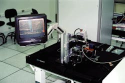
The first of the process-control tests, the broad-area test, is performed immediately after crystal growth. Its primary purpose is to provide fast feedback on the quality of the layers grown (see Fig. 1). Typical measurements include threshold-current density, the slope of the light intensity versus forward current curve (L/I curve) to assess device efficiency, and the spectral characteristics of the laser (center wavelength and bandwidth). If these are not all within specification, there is no point in expending further time and money to process the wafer.
Fabrication of broad-area lasers involves metalizing both sides of the wafer to provide the electrical contacts for driving current through the laser diodes. Stripes are defined on the top contact through photolithography or by using a shadow mask during metal deposition. The wafer is then cleaved into laser bars for probing.
The test instrumentation consists of an automated system capable of measuring five bars simultaneously to maximize throughput. Bars are placed into the test fixture and manual actuators are adjusted to position the first contact pad under the probe tip. A built-in video system aids the operator in accomplishing this.
With the bars in place, the rest of the test is automatic; motorized actuators index the wafer, sequentially aligning the contact pad of each laser under the probe tip. This probe tip is raised and lowered by motorized stages. Because the device architecture does not yet include current confinement, a fairly high current (1 to 3 A) is driven through each device to achieve lasing action. In contrast, the final lasers will operate typically with only a few hundred milliamps. A pulsed driver prevents this high current from causing resistive heating and consequently thermal damage to the laser. A thermoelectric cooler allows the testing to be conducted over a temperature range of 20°C to 65°C.
Output from each laser is collected by an integrating sphere with two measurement ports. The first port contains a photodiode for measuring laser output power. This is combined with the current data from the driver to construct the L/I curve. The other output port contains a fiberoptic cable that sends a small sample of the light to an optical spectrum analyzer that determines the laser center wavelength and bandwidth.
Laser-diode bar test
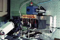
The next important test occurs after wafer processing is complete and the wafer has been cleaved into bars. The laser diode holding and positioning hardware in the laser-diode bar-test instrumentation is essentially the same as that used for the broad-area test. But, because device processing is complete, the lasers are driven by a constant-current laser diode driver (see Fig. 2).As before, an integrating sphere provides an output power reading; forward voltage (V) is tracked so that the complete L/V/I characteristics of the device can be assessed, from which the threshold current, slope efficiency, and series resistance are measured. Kinks in the L/I curve—points at which the slope of the L/I curve deviates from a linear behavior—are identified using an aperture in front of the integrating sphere, and the device is rated with the current or output power below which it is kink-free. Kinks must occur only above the specified output power in order for the device to pass this test. Again, an optical spectrum analyzer provides the center wavelength and spectral bandwidth.
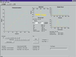
The laser-diode bar test also collects spatial measurements of the laser diode output. After the first set of measurements is made, the bar is moved, and a second probe tip makes contact. This output is directed to a beam profiler for near- and far-field beam measurements (see Fig. 3). During this test the diode is again actively temperature-controlled by a thermoelectric cooler in the range of 20°C to 65°C, so that each parameter can be characterized as a function of temperature.Chip-on-carrier burn-in
After the bars have been diced and the individual lasers mounted on their ceramic subcarriers, the chip-on-carrier (COC) burn-in is performed. Up to
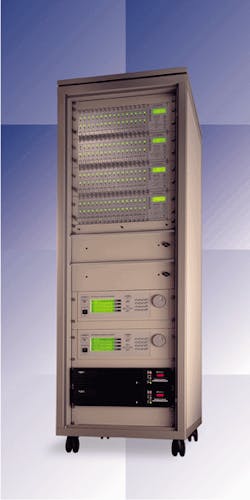
16 separate lasers are loaded on to a removable fixture specially designed by Newport (see Fig. 4). The fixture also contains photodiodes for measuring the output power from each laser, as well as thermoelectric coolers capable of maintaining the temperature of the fixtures anywhere in the 20°C to 85°C range. The COC burn-in station utilizes standard laser diode drivers to run the lasers in either a constant current or constant power mode; an uninterruptable power supply is also included.The COC burn-in is run for about 300 hours while lasers are monitored to identify any devices with output power that drops a predetermined amount. Operating at an elevated temperature shortens this burn-in time and helps stabilize the lasers as well as weeding out devices subject to "infant mortality" or those damaged during the bonding process.
Module pretest
After the laser is bonded to a thermoelectric cooler, photodiode monitor, and impedance-matching circuitry, it is subjected to a module pretest. The goal of this test is to establish that the thermoelectric cooler was not damaged during the bonding process. If there is a problem with the cooler at this stage, it is still possible to remove and reuse the other device components. After fiber alignment, however, any problems will require scrapping the entire device.
The test involves a series of voltage and current measurements at various temperatures on the thermoelectric cooler to calculate its dynamic resistance. Results are compared to a pre-established pass/fail window. The electronics for this test include two temperature controllers and a custom mount developed by Newport; custom software controls the test and acquisition of cooler voltage and current data.
Final tests
Once the fiber is aligned and the module is hermetically sealed, a final series of temperature cycle and burn-in tests is conducted. These culminate with the module burn-in—identical to the chip-on-carrier burn-in with the exception that different fixturing holds the butterfly-packaged lasers; eight lasers are held on a single fixture. During this burn-in, laser output is monitored while the module is maintained at an elevated temperature (60°C to 80°C).
The final module test assesses virtually every aspect of device performance. The module test station characterizes two lasers at a time and is based on standard laser-diode current supplies and thermoelectric-cooler controllers. Using a fiberoptic switch, the fiber output from the laser diode can be sent to an integrating sphere for complete L/V/I characterization or to an optical spectrum analyzer for wavelength and linewidth measurement. Varying the external temperature range from -20°C to +85°C while holding the thermoelectric cooler between +20°C and +30°C allows verification of the cooler operation and ensures that any thermally induced kinks in the L/I curve remain above the maximum rated power at all operating temperatures. Comparing the fiber output with that of the internal monitor photodiode allows any temperature-dependent fiber misalignment or packaging-induced effects to be identified.
All of the test instruments described here are networked together so that results for a given laser can be tracked and documented through the entire manufacturing process. Thus, output parameters can be compared before and after each manufacturing stage, allowing rapid identification of any packaging-related problems in a specific unit. Statistical analysis of these data further aids in pinpointing any process-related problems.
As the use of fiberoptic telecommunications systems grows, there is increasing demand for both higher-reliability and lower-cost components. Laser diode manufacturers, working together with instrumentation vendors, have responded to this need with a range of automated test equipment that is enabling better process control and more-thorough device characterization in a volume production environment.


