Integrated FTIR reflectometer controls semiconductor fabrication process
PETER ROSENTHAL
The semiconductor industry has been driven by a trend toward larger wafers with a higher density of devices with smaller features. Though the cost to manufacture integrated circuits on a per-device basis has been historically decreasing, the cost per wafer has been rising dramatically. A modern 200-mm wafer when processed can represent up to $100,000 in finished goods. As the industry moves to adopt 300-mm-diameter wafers, the value per wafer is expected to increase even more.
The increasing cost and complexity of the manufacturing process is bringing about a shift in the role of metrology from off-line statistical sampling to in-line process monitoring and control, in which the product wafers themselves are measured nondestructively to monitor the process. The benefits of in-line measurement and control will be most fully realized when the metrology tool is integrated directly onto the semiconductor fabrication tool, allowing measurement and closed-loop process control with a minimum delay between the process and metrology steps. Integrated metrology has the additional advantage of providing rapid detection of process excursions and reactor faults, which will reduce the numbers of out-of-specification wafers that must be scrapped.
The ideal integrated sensor would have several features. It would be a noncontact, nondestructive, physically robust tool that provides a key semiconductor measurement needed to monitor or control an important process step. To be used in a production environment, the sensor must be capable of operating reliably 24 hours per day with minimal user interaction. Optimally, measurement, control, and data archiving would be fully automated and integrated with any factory-wide manufacturing execution system software.
Optical materials characterization techniques are well suited to integration into process-control systems because they are nondestructive, noninvasive, and able to probe a wide variety of ambient gases and liquids through optical windows. Infrared spectroscopy has some particular advantages for semiconductors when information about the materials electronic properties and composition is desired in addition to layer thickness. Furthermore, for the case of epitaxial silicon, thickness measurements are not possible using visible and ultraviolet wavelengths.
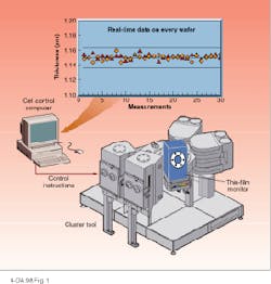
Optical metrology techniques offer a practical approach to integrated metrology on the semiconductor line. On-Line Technologies (East Hartford, CT), with Applied Materials Inc. (Santa Clara, CA), has developed a compact Fourier-transform infrared (FTIR) thin-film monitor for measurements of semiconductor thin films for integration into commercial semiconductor process tools (see Fig. 1). The thin-film monitor is mounted on a multichamber epitaxial silicon chemical vapor deposition cluster tool that consists of two load locks, a central transfer robot, two process chambers and a cooldown chamber. The thin-film monitor sits on top of the cooldown chamber, with an infrared window allowing optical access to the wafers for the measurements.
During epitaxial deposition, the wafers are processed one at a time. In a typical process sequence, the transfer robot transports a wafer from a cassette in the load lock to one of the process chambers, where the epitaxial layer is deposited. The film is grown at high temperature (~1100°C) through a reaction with a flow of a silicon-containing precursor gas. The entire process is computer controlled via a “recipe” that directs the cluster tool to configure the various setpoints for temperature, pressure, flow, and other parameters that characterize the process. After the deposition, the wafer is transported by the transfer robot into the cooldown chamber, where it cools for approximately one minute. During the cooldown, the film thickness monitor makes a measurement of the film thickness. After the cooldown and measurement steps, the wafer is returned to the cassette in the loadlock. The thickness data from the sensor are used in a run-to-run feedback control loop, in which the recipe is modified between wafers to correct for any observed drifts in the process. Warnings also are issued if the process drifts outside of predetermined control limits.
System design
The sensor consists of an FTIR spectrometer configured to perform a reflectance measurement. The spectrometer is a dual-path (Michelson) interferometer configured to simultaneously modulate blackbody infrared radiation, white light, and a laser beam. The modulated white-light source provides a sharp intensity peak that calibrates the zero-path difference (ZPD) position of the moving mirror in the interferometer. The modulated laser provides fringes that are used to trigger the data acquisition system at a uniform calibrated spacing in retardation. The blackbody (or glow bar) provides a broadband infrared signal that is sampled as an interferogram. The raw interferogram data are collected as intensity vs. mirror retardation position relative to ZPD.
As the mirror sweeps through an interferogram, each wavelength of light from the glow bar goes through cycles of destructive and constructive interference at a rate proportional to the optical frequency. For example, radiation at 5 µm in wavelength will undergo twice as many interference fringes as will light of 10 µm in wavelength for any given mirror sweep. Each infrared frequency is thus encoded in the interferogram with a unique amplitude modulation frequency. A fast-Fourier transform (FFT) of the interferogram then yields the optical spectrum of the infrared beam.
To measure reflectance, sampling optics are provided that allow the beam to be detected after being reflected from the surface of the wafer or some reference sample. The spectra from the wafer, in ratio to the signal reflected off a calibrated reference surface, allow calculation of the reflectance.
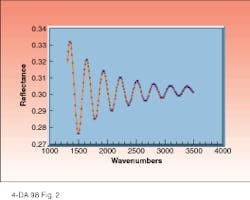
In a wafer, typical of commercial epitaxial silicon, the epitaxial layer is lightly doped, while the substrate is heavily doped. The infrared reflectance spectrum shows a fringe decaying toward higher frequencies. This fringe is due to interference between the light reflecting from the film surface and the light reflecting from the film/substrate interface. In the case of epitaxial silicon, where the substrate and the film are both silicon, the only difference between the layer and substrate lies in their free-carrier concentrations. The free carriers in doped silicon have a significant contribution to the index of refraction in the mid-infrared wavelength range, hence the observed interference fringe. In contrast, the doping has a negligible effect on the visible and near-IR optical properties of silicon, and no fringes are detectable using visible spectroscopy.
The fit of the measured reflectance spectrum employs an accurate model for the frequency and doping dependence of the complex index of refraction of the silicon (see Fig. 2). The modeled doping profile is varied iteratively during the fitting process to match the measured reflectance. The software then computes the layer thickness and interface diffusion length from the fitting parameters. The sample shown has a layer thickness of 5 µm, with a film substrate interface approximately 0.3 µm wide. Using this model-based analysis algorithm, the epitaxial film thickness can be determined with a relative precision of approximately 1 nm in film thickness, and an intermachine reproducibility of approximately 3 nm. The FTIR measurements also correlate well with destructive depth-profiling techniques such as secondary ion mass spectroscopy (SIMS), with the agreement being within 20 nm—the precision limit for SIMS.The data acquisition, spectral analysis, and feedback control to the cluster tool were all implemented on a PC running LabView (National Instruments; Austin, TX). The model-based analysis algorithms are extremely flexible and have been applied to integrated measurements of other process steps involving polycrystalline silicon, oxide layer formation, and layer etch. Future applications extend these and other processing steps and include the capability for multipoint measurements on the cluster tool to provide control of wafer uniformity.


