Imaging ellipsometry analyzes small samples
Imaging ellipsometry analyzes small samples
Decreasing device dimensions and increasing complexity of multilayered structures demand improved spatial resolution.
Dirk Hoenig
The recent development of imaging ellipsometry opens up the possibility of reducing measurement times and creating new possibilities for structured films. The technique is based on a century-old process of ellipsometry--a very sensitive, nondestructive optical method of characterizing surfaces and thin films. Ellipsometry analyzes the change in the state of polarization of a light beam reflected or transmitted by the sample and is mainly used for the determination of film thicknesses ranging from nanometers--monolayer coverage or below--up to a few microns. In the semiconductor industry, ellipsometry is a standard metrology tool for measurement of thin films.
Basic ellipsometry principles
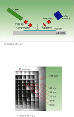
As many important ellipsometry applications include the use of opaque substrates, a V-shaped, reflective instrument tends to be most common and has been carried over to the design of the imaging ellipsometer (see Fig. 1). In classical ellipsometry, the parallel (p-) and perpendicular (s-) polarized components of the incident lightwave exhibit multiple reflections inside the film/substrate system. Reflection and transmission coefficients at the interfaces account for the amplitude of each partial wave, as well as phase jumps at the interfaces and phase shifts due to the optical paths that the waves have to travel. The angle of incidence and the film thicknesses are the geometric parameters, while the complex refractive indices account for the material properties of the media involved. This analysis becomes more complicated if the media are optically anisotropic, optically active, magneto-optic, or of an unpleasant nature in any other way.
The resultant emitted lightwave is a superposition of all partial waves, thus carrying information about the integral effect of the total film/substrate system under study. In general, a film/substrate system will change a certain elliptical polarization at the input (incident beam, including linear or circular polarization in special cases) into a different elliptical polarization at the output (reflected beam). This change is described by two real quantities, where psi denotes the change of amplitudes of the p- and the s-polarized component while delta gives their relative phase shift upon reflection. Psi and delta at a given wavelength are the two quantities measured by most standard ellipsometer designs.
There are powerful and elegant methods to calculate the interaction of a lightwave with different kinds of samples, especially with multilayered film structures.1 Thus, it is relatively easy to simulate the measurable quantities psi and delta for a specific type of ellipsometer. However, the inversion of the equations to get the desired physical quantity, such as the film thickness, from an ellipsometric measurement is usually not possible in an analytic form. Therefore, numerical regression algorithms must be applied (see "Classical ellipsometry," p. S38).
A significant challenge in thin-film metrology arises for laterally structured samples, such as on processed wafers in the semiconductor industry. A traditional HeNe laser beam of a standard ellipsometer with its 1-mm spot diameter or the even larger spots of spectroscopic ellipsometers require large probing areas or unpatterned monitor wafers. This obviously is disadvantageous, so that options have been developed by many companies to focus the beam onto the sample. Still, this limits the probing area diameter to typically 50 µm because of the nonideal light source in spectroscopic ellipsometers. Especially when new processes or new thin-film materials are evaluated, a higher lateral resolution is desired, because during the early stages of development the resulting thin films will often be inhomogeneous. For the wide field of applications where an intrinsic structure on the micron scale is a desired feature of the sample--when optical properties of magnetic domains are studied, for example--a high lateral resolution is also needed.
Enter imaging ellipsometry
A new approach to this problem is imaging ellipsometry. Here, the incident light is still a collimated laser beam, but an imaging system on the detection side accounts for the lateral resolution. By applying this technique, the dimensions for the probing area can be reduced by an order of magnitude compared to the focusing options of non-imaging systems. For imaging ellipsometry, the classical configuration of nulling ellipsom- etry can be chosen. Besides its high sensitivity, this method offers a very direct and clear approach to ellipsometry--rotate a polarizer (P) and a quarterwave plate (C) to modify the polarization of the incident light beam in such a way that the beam reflected from the surface (S) exhibits a purely linear polarization.
When an analyzer (A) is rotated at 90 with respect to this linear polarization, no light reaches the detector. The ellipsometric null is obtained. Now, putting all the rotation angles of P, C, and A into the mathematical model that describes the optical behavior of the sample, it is possible to deduce parameters of the sample. To build an imaging ellipsometer from this nulling ellipsometer configuration one needs a spatially resolving detector (CCD camera) and an imaging system. This can be a long-working-distance microscope objective that produces an image of the illuminated area on the detector.
The advantage of choosing the nulling ellipsometer configuration is the ellipsometric contrast it generates for inhomogeneous, laterally structured samples--while one region of the sample may appear dark for a given setting of P, C, and A, another region of different optical properties (such as film thickness) will appear bright. This allows ultra-sensitive surface inspection at real-time video rates. Surface defects, scratches, and monolayer-thin contaminations become visible as well as desired structures like a patterned thin film. As the next step, one can use the camera signal for quantitative ellipsometric analysis. By defining regions of interest and averaging the gray level within a particular region with the help of a frame grabber and dedicated image processing software it is possible to perform (automated) nulling ellipsometry within the selected region only. To increase the limited dynamic range of the camera, electronic shutter and laser power control can be applied.
It is now possible to do local ellipsometric analysis on a surface structure as small as a few microns (see Fig. 2). While the resolution of the real-time ellipsometric contrast imaging is related to the numerical aperture of the objective used, the resolution for the analysis is primarily limited by the signal-to-noise ratio of the detector, which will usually make it necessary to average over several camera pixels. However, another limitation arises from the fact that for small structures with dimensions in the range of the wavelength, the assumption of a plain incident wave in the standard optical models is not valid.
Besides single-point measurements on selected sample areas it is also possible to map the image field, which yields a 3-D surface topography. Instead of the time-consuming point-by-point scanning, as in conventional film-thickness wafer mapping, the imaging method allows parallel processing for a speedy mapping on the microscopic scale. Multiple-wavelength operation via an optical fiber extends the capability of the instrument to the analysis of multilayered film structures.
Overall, there are two major advantages of imaging ellipsometry compared to standard ellipsometry. Due to the ellipsometric contrast, rapid surface inspection with unrivaled sensitivity to surface contamination, defects, and film homogeneity becomes possible. And the ellipsometric analysis can be restricted to areas of only a few microns, allowing new applications for laterally structured samples. Future developments in this area will include construction of imaging spectroscopic ellipsometers to increase the analytical capabilities and large-area imaging ellipsometers for the semiconductor or flat-panel display industry, thus allowing the imaging of the entire surface of 300-mm wafers at one time. This may speed up film-thickness mappings by one to two orders of magnitude. o
REFERENCE
1. R. M. A. Azzam and N. M. Bashara, Ellipsometry and Polarized Light, North-Holland Physics Publishing.
FIGURE 1. In imaging ellipsometry the V-shaped reflective structure often used in classical ellipsometry is maintained, but the imaging ellipsometer includes a CCD camera detector and an imaging system.
Classical ellipsometry
Two traditional methods of determining physical parameters of thin films involve numerical regression algorithms. One is based on a single wavelength of light, the other on multiple wavelengths.
Single wavelength ellipsometry
From a single-wavelength, single-angle-of-incidence measurement, in principle, two real physical parameters can be derived. This means, that a single isotropic, nonabsorbing film on a known substrate can be analyzed with respect to film thickness d and refractive index n with one single ellipsometric measurement, unless certain restrictions apply. If there are more unknown parameters--such as extinction k, substrate n and k, or multilayered films--it becomes necessary to increase the number of independent measurable quantities. This can be achieved by performing measurements at multiple angles of incidence, which also helps to resolve the problem of the periodicity of the ellipsometric parameters for films that are thicker than roughly half the wavelength of the probing light.
Multiple wavelength and spectroscopic ellipsometry
Especially in the semiconductor industry, thin films are produced in a multitude of processes and for various purposes leading to very complex multilayered film structures on the (silicon) substrate. To be able to analyze such complicated film structures it has became popular to apply multiple-wavelength ellipsometry or spectroscopic ellipsometry where psi and delta are recorded over a wide range of wavelengths. The dispersion of n and k for each film produces a characteristic dependency of psi and delta as a function of the wavelength for a given film thickness. The complicated psi/delta spectrum can be seen as a unique fingerprint of the sample. Because a psi/delta spectrum gives double the information compared to a spectrophotometric measurement (where the reflectivity is measured), along with a higher resolution, it is evident that this method is superior for the analysis of either very thin or very complex film structures or films with low reflectivities. Today`s commercial spectroscopic ellipsometers, for example, those from Woollam (www.jawoollam.com) or Sopra (www.sopra-sa.com), use sophisticated computer algorithms to derive film thicknesses and many other parameters from spectroscopic, multiple-angle measurements.
FIGURE 2. Illumination through a square mask with a strong UV laser pulse led to ablation of a spincoated photoresist on an Si wafer. Imaging ellipsometry determines the film thickness for each individual square and the ellipsometric image reveals that the illumination mask is not homogeneous, as can be concluded from the brightness gradient within each square.


