Surface Analysis: New metrology tools support MEMS from R&D through final QC
Patricia Browne and F. Michael Serry
Microelectromechanical systems (MEMS) are used in a wide range of applications, from digital light processing (DLP) chips for projection televisions to “lab on a chip” microfluidic devices for high-throughput proteomics. Successful MEMS device operation is critically dependent on the dimensions, surface quality, and precise motion of its parts, which creates a need for numerous accurate measurements at many stages of MEMS development, from R&D through production.
Three different metrology methods that meet this critical need are optical profiling (white-light interferometry), stylus profilometry, and atomic-force microscopy. One reason these particular techniques have been so widely adopted is that each one provides simultaneous measurement of multiple parameters-flatness, roughness, xyz dimensions, and so forth.
Optical profiling
White-light interferometry (optical profiling), relies on a unique type of optical microscope with epi (through the objective) illumination from a broadband filtered lamp source. The objective contains a beamsplitter that focuses half of the light onto the sample and half onto an extremely high-flatness reference plate-a configuration that produces interference fringes in the recombined light, which are recorded by a CCD camera. But because the broadband light source has extremely low coherence, fringes can only be formed when the path difference in this interferometer is virtually zero.
In operation, the microscope objective continuously scans through a range of focal positions. The instrument’s software then calculates the z (vertical) surface dimensions at low resolution by noting the focal position that produces the highest contrast fringes. This delivers z-axis dimensional resolution at the subnanometer level.
The lateral (xy) resolution of the profiler depends on the magnification and field of view of the objective; instruments are usually supplied with a selection of different objectives. At the highest magnification, the lateral resolution is about 0.5 µm. The z-axis resolution is unaffected by changes in magnification. Originally for measuring semiconductor wafers, these instruments are now used for a diverse range of MEMS measurements from the depth of a microfluidic etched channel, to the roughness of a channel or mirror surface, to the bow in a cantilever.
The initial popularity of optical profilometry in MEMS resulted from a unique combination of benefits. First, this is an imaging technique that provides area measurements with more than 300,000 xy data points collected simultaneously. Second, this technique simultaneously measures three dimensions, quantifying roughness, feature size, and other topographic metrics for MEMS devices. In addition, the instrument software can be readily programmed to perform automated pass/fail tests on critical dimensions at multiple locations.
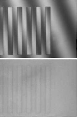
However, two recent advances make optical profilometry even more powerful for characterizing and measuring MEMS. The first of these-dynamic MEMS (DMEMS)-uses stroboscopic interferometry to image and analyze device motion in real time. In a DMEMS-equipped optical profiler, a high-brightness LED provides light that is strobed according to an input reference signal. The effect is to create a “stopped motion” view of the device under test. Moreover, the phase of strobing can be adjusted (or swept) to capture the position and shape of a moving part at any phase of its movement cycle. Most important, the introduction of DMEMS in no way compromises the instrument’s resolution or ability to perform multidimensional metrology and surface analysis. In use, DMEMS can identify defects that would otherwise be invisible during a static test (see Fig. 1).
The second advance is the ability to perform measurements through transmissive media (TTM), such as windows or other clear packaging. Until 2005, such capability was limited, which created difficulties with final QC of devices that are enclosed with dry nitrogen (or other gases with properties different from ambient air). It also prevented testing in an environmental chamber.
To accomplish TTM measurement, a new type of microscope objective (patent pending, Veeco Instruments) was engineered to accommodate a preregistered slot for simple insertion (and removal) of a range of transmissive compensation plates. A piece of material identical to the packaging or chamber viewing window is inserted in the reference arm of the interferometer to cancel the optical effects of the MEMS package window. Using a shaped, narrowband illumination source both static and DMEMS measurements can be made at up to 40× magnification through windows up to 3 mm thick (see Fig. 2).Atomic-force microscopy
The atomic-force microscope (AFM) is the ultimate tool for extremely small-scale three-dimensional surface measurements, delivering resolution down to the atomic level. In an AFM, a fine tip at the end of a microfabricated cantilever is moved with piezoelectric actuators, bringing the tip into perpetual or intermittent contact with the surface. The movement of the cantilever as the tip scans the sample surface is measured by reflecting a collimated laser beam off the top surface of the cantilever, and monitoring the reflected beam with a position-sensing photodetector.
For surface morphology, the instrument can be operated in a continuous contact mode or in an intermittent contact “tapping” mode. Today, most surface morphology is carried out using a tapping mode, in which the cantilever is maintained in constant-amplitude oscillation, typically around 10 to 50 nm rms. This enables the tip to be rapidly scanned across the test surface while reducing drag artifacts or damage to the tip or surface that arise from shear forces during perpetual contact scanning.
One of the main advantages of the AFM is its three-dimensional resolution-typically nanometers in the xy plane and angstrom or better in the z direction. Moreover, unlike the optical profiler, AFM performance is independent of the optical properties of the subject. Conversely, however, the AFM cannot perform metrology through package windows.
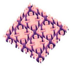
A key early industrial MEMS application for the AFM was in Texas Instruments’ development of the now ubiquitous DLP chip used in projection TVs and data projectors. Here the planarity of the mirrors and their actuators is critical to proper function, but these components are so small there was no other tool that could do the job as well as the AFM (see Fig. 3). Furthermore, these DLP-type devices continue to shrink, as does the separation between the mirrors.Atomic-force microscopes continue to prosper in this and other MEMS applications because the core technology is flexible enough to be configured for both R&D and statistical on-line QC, supporting volume production. Indeed, manufacturers now often make extensive statistical measurements at each separate stage of production to maximize yields. These on-line tools are characterized by a high level of automation, including hands-free exchange of both the tip and the sample when desirable. In addition, powerful software reduces the data to usable information in the form of meaningful statistical process parameters.
MEMS applications of the AFM are being driven by another key advantage of the instrument, namely its ability to go beyond precision metrology and to characterize electromechanical performance. These applications-generally categorized as nanotribology-utilize various aspects of the interaction between the probe tip and the sample, including the ability to measure the vertical and horizontal manifestation of the adhesive force between the tip and the sample surface.
Stylus profilometry
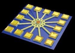
Stylus profilometry predates many other types of surface metrology techniques, yet it continues to enjoy robust market share, particularly in the area of MEMS. As its name suggests, the technique relies on a fine mechanical stylus that contacts the test surface under slight positive pressure. The test sample is then translated in the horizontal (xy) plane relative to the stylus. Surface variations cause vertical motion of the stylus that is detected by a high-performance inductive sensor at the end of a lever arm. In this way the instrument builds a line-transect profile of the surface (see Fig. 4). A full three-dimensional profile can easily be recorded by xy raster motion of the surface.Stylus profilometry is micromechanical and therefore does not require the measurement of the optical properties of the films, layers, and microdevices. It is also the fastest method of obtaining a long-line sample across a MEMS wafer-up to 100 mm in a single scan (up to 200 mm stitched) taking only 60 seconds. Moreover, stylus profilometry provides high-repeatability data in all three dimensions with high dynamic range and resolution. Specifically, a high-performance instrument can provide a z-measurement range up to 1 mm with a vertical resolution of 1 Å. And the latest high-resolution tips can provide lateral (xy) resolution at the sub-100 nm level. So, this well-established technique can simultaneously deliver 3‑D metrology while providing accurate surface-roughness measurements.
Another advantage of stylus profilometry is its relatively modest cost, making it a popular technique for on-line process monitoring where multiple metrology stations can be required. For instance, stylus profilometry has now attained a dominant position as the preferred method for process control of film-deposition equipment in MEMS, which is one of its main MEMS applications-the instruments are also durable and long-lived, which further maximizes their performance/cost ratio.
The technique’s popularity in MEMS is a result of these benefits together with recent advances specifically targeted at MEMS applications. The introduction of super-sharp styli that can fully characterize submicron lines and spaces, for example, plus the availability of high-aspect-ratio tips to probe deep structures as well as to measure shallow-trench-isolation (STI) etch depth. In addition, the fast line-transect capability supports a common MEMS fabrication requirement, namely to measure the compressive (or tensile) stress across a wafer after deposition of film(s).
Another advance has been development of low-force stylus sensors, which addresses one of the drawbacks of earlier stylus instruments-the possibility of scratching softer surfaces, which is undesirable for nondestructive testing applications, particularly with MEMS wafers that often incorporate relatively soft layers. The latest MEMS-targeted instruments diminish the impact of contact forces by offering stylus forces equivalent to 0.03 mg gravitational mass. And finally, software protocols have been optimized specifically to provide 3-D data analysis for surface characterization of MEMS.
Despite the different underlying technologies of these popular metrology methods, there are both overlapping and complementary aspects of their capabilities. Therefore, when choosing which technique to use, it is vitally important to discuss specifics of the intended application with an experienced instrument vendor to ensure the optimum solution is selected.
PATRICIA BROWNE is marketing product manager and F. MICHAEL SERRY is senior applications scientist at Veeco Instruments, 2650 East Elvira Road, Tucson, AZ 85706-7123; e-mail: [email protected]; www.veeco.com.


