SPECTROMETRY: CCD spectrometer folds spectral images from 200 to 1000 nm
In traditional spectrometers, grating or prism dispersion elements are rotated continuously in fine steps using a mechanical mechanism to scan the wavelength and achieve high-resolution spectral measurements. Although 2-D silicon-based charge-coupled-device (CCD) or complementary-metal-oxide-semiconductor (CMOS) detector arrays have been used to record many spectral lines at the same time in parallel data-acquisition mode, the effective spectral-measurement range is only 80 nm for a 26.8 × 28-mm CCD array for a dispersion of 3 nm/mm. But, using a special grating consisting of ten subgratings, researchers in the Department of Optical Science and Engineering at Fudan University (Shanghai, China) have succeeded in developing a high-resolution CCD spectrometer that folds dispersed spectral images ten times, without any mechanical moving parts, to cover the full 200- to 1000-nm working wavelength range with an acquisition time of less than 100 ms.1
The secret to the spectrometer system is its unique grating, designed to arrange ten spectral zones with different wavelength windows covering the 200-to-1000-nm range in sequence along the direction perpendicular to the spectral distribution, to fill the image plane of the 26.8 × 28-mm CCD array. The integrated grating structure consists of 10 subgratings at different angles of incidence, each with a density of 1200 grooves/mm. Each subgrating is approximately 60 × 5 mm, with the grooves parallel to the short side.
In the experimental setup, the grating was placed within an optical cavity that focused the light from a mercury (Hg) lamp to the focal plane of the CCD. The optical path sent the light from the entrance slit to a plane mirror, to a spherical mirror, onto the grating, and then to a toroidal mirror before reaching the CCD. The entrance slit was fabricated from eight 125-µm-diameter silica fibers, arranged to form a spot-to-slit fiber bundle with a slit length of approximately 1 mm.
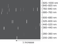
For the CCD array with 1340 × 1300 pixels, each approximate 80-nm wavelength zone was imaged to a 1340 × 130-pixel region of the CCD. Spectral lines from the Hg lamp were imaged to the CCD, with ten clearly defined spectral regions corresponding to the ten subgrating regions (see figure).
To correct for any dispersion errors, a polynomial function was used to fit the wavelengths to the pixel positions for each of the ten grating regions in a calibration procedure that used a standard 0.5-m-focal-length monochromator. Although the pixel position is not exactly linear to the wavelength, the error is small from 200 to 1000 nm because each individual wavelength region is imaged on a narrow physical region of about 7°. Using the calibrated wavelength-to-pixel curves in the measurement, the calculated spectral resolution is approximately 0.065 nm/pixel over the full wavelength range. Experimental determination of the spectral resolution by measuring the full width at half maximum of the spectral line from a HeNe laser yields a value of 0.12 nm; that is, wavelengths with a separation of 0.12 nm are easily resolved.
“The CCD or CMOS array detector spectrometer is a revolutionary design-it will become a mainstream technology and a trend in modern optical-spectrometer design to have a densely folded image by using multiple gratings to realize measurement in the wide spectral range with high speed, high resolution, and long-term reliability,” says Hai-Ling Yuan, senior optical scientist and professor from the Shanghai Institute of Measurement and Testing Technology (Shanghai, China).
REFERENCE
1. Y.-R. Chen et al., Optics Express 13 (25) 10049 (Dec. 12, 2005).
About the Author

Gail Overton
Senior Editor (2004-2020)
Gail has more than 30 years of engineering, marketing, product management, and editorial experience in the photonics and optical communications industry. Before joining the staff at Laser Focus World in 2004, she held many product management and product marketing roles in the fiber-optics industry, most notably at Hughes (El Segundo, CA), GTE Labs (Waltham, MA), Corning (Corning, NY), Photon Kinetics (Beaverton, OR), and Newport Corporation (Irvine, CA). During her marketing career, Gail published articles in WDM Solutions and Sensors magazine and traveled internationally to conduct product and sales training. Gail received her BS degree in physics, with an emphasis in optics, from San Diego State University in San Diego, CA in May 1986.
