OPTICS FABRICATION: Subsurface damage is measured nondestructively
KEVIN R. FINE, REINHOLD GARBE, TUNG GIP, AND QUOC NGUYEN
Subsurface damage such as cracks, voids, and contaminant particles are a fact of life in even the highest quality optics. The damage can be inherent to the type or quality of the material used, or it can be produced during sawing, grinding, polishing, and other fabrication steps. Regardless of the source, the amount of damage determines an optic’s yield strength, the flatness that can be maintained during coating, and the amount of laser power that the component can safely handle.
In precision optical elements, such damage can present considerable risks of performance irregularities and even system failure, particularly in applications that involve either significant physical stresses or the use of high-power laser light. When these conditions are present and the cost of failure is high, any problems caused by subsurface damage become critical. For instance, subsurface damage in an optical path that causes light absorption and scattering can lead to poor-quality optical signals or heat generation that in extreme cases can cause the optical element to explode.
Subsurface damage also plays an underappreciated role in meeting quality requirements. In an optic that appears to be within specifications at the end of manufacturing, subsurface cracks often propagate once the optic is exposed to the heat of the coating chamber. These cracks lead to warping, making it nearly impossible to meet tight wavefront and flatness requirements.
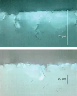
Unfortunately, surface-profile measurements alone can yield extremely misleading answers because there is no predictable correlation between quality on the surface and quality within the component. One sample can have a smoother and flatter surface overall than another sample, for instance, but also have more extensive subsurface damage (see Fig. 1).
To bring some certainty to the fabrication process, various mathematical models have attempted to assess the quality of the optical element based on knowledge of the materials and fabrication processes utilized. An accurate model could conceivably determine the expected damage in a particular design. However, such models will be inaccurate if the model is based on inaccurate characterizations of the material or the fabrication process, or if effects not anticipated in the model cause damage. Furthermore, even when a model is accurate, the level of subsurface damage in individual optical elements is generally subject to variations, and a specific element may have more or less subsurface damage than expected.
Without a simple and reassuring way to assess quality or obtain accurate feedback during fabrication, processes are generally developed based on beliefs and rules of thumb, rather than on dependable information. For instance, glass fabricators start with coarse grit, which removes material quickly but causes deep cracks. The next step is to move to a finer grit and machining long enough to remove the material to the depth of the cracks made with the coarse grit. This process is then repeated with ever-finer grits. However, without accurate knowledge of the depths of whatever subsurface cracks are in the piece, fabricators more or less end up guessing how long to machine each piece. The result is either suboptimal parts or suboptimal processes—or both.
Existing methods
Given the costs and risks of poor quality, numerous attempts have been made to develop efficient and reliable methods of detecting and assessing subsurface damage. The most common techniques fall into two general categories: destructive measurements and measurements of scattered light.
In destructive measurements, a test sample is physically modified, such as through grinding or acid etching, to expose material below the surface. These techniques can be used to build a model of either the materials or the fabrication processes. However, each optical element evaluated in this manner is generally rendered unusable, which is obviously undesirable with expensive components. Also, because destructive evaluation is usually a sampling process, it measures only typical subsurface damage for a given design subjected to a given process. Consequently, some uncertainty always exists regarding those units that weren’t evaluated. Further, the results of a destructive evaluation can typically take several days to obtain.
In measurements of scattered light, laser light impinges on the surface at an angle, and a detector is positioned to receive backscatter resulting from subsurface damage. A horizontal scan is performed and the intensity of the backscatter recorded at each location on the horizontal plane. The intensity is then correlated with depth through a lookup table, resulting in estimates of subsurface damage. However, no direct vertical depth measurement is made.
Among the other methods that have been tried, acoustic measuring techniques examine the surface condition and fracture toughness of an optical element, but they have trouble detecting defects larger than about 10 µm. In addition, they require expensive equipment and a significant amount of skill, training, and technical support.
Direct, nondestructive measurements
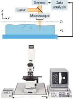
A new nondestructive technique that combines direct subsurface measurements with real-time graphical analysis has proved effective in overcoming the drawbacks of existing techniques. This method adapts a confocal scanning laser microscope system typically used in surface-scanning applications (such as assessing surface topographies of platters in optical disk drives) but directs the focal plane into the optic element, rather than scanning the surface (see Fig. 2).The focal plane of the microscope is adjusted vertically to various depths within the optical element. Given the ability of a confocal microscope to block returned light from above and below the focal plane, this approach achieves visual resolution of 150 nm up and down the vertical axis (in the case of the microscope in the implementation shown). The system conducts a 3-D internal scan of the test article through optical sectioning, stacking a collection of horizontal focal planes between the minimum and maximum depths set for the test. A complete 3-D profile is created in a matter of seconds for a typical optical element, providing the real-time answers needed to ensure product and process quality.
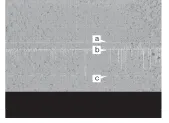
At each observation point within the test zone, an increase in the intensity of reflected light indicates scattering or reflection from a defect or damage at that point within the component. The area over which defects extend and the intensity of the light indicates the severity of the damage.
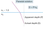
Because a scanning laser microscope is intended for measuring surface features, once the microscope penetrates the optical surface, the material’s index of refraction causes the apparent depth to differ from the actual depth (see Fig. 3).Looking at the graph, we can then position a measurement cursor (c) at the deepest valley, as indicated by the numerical readout of 127.23 µm. To convert this observed depth to the actual depth, we follow the refractive-index-based scaling procedure to accommodate refraction. The fused-silica material used in this particular test, for instance, has an index of 1.47 at this wavelength, yielding an actual depth of 187 µm.
This new technique for measuring subsurface defects and damage has already helped Agilent optimize and characterize its manufacturing processes to create optics with the desired level of subsurface integrity. The close correlations observed in experimental comparisons between this new approach and conventional destructive test methods on a variety of samples offer a new level of confidence in the performance and dependability of optical elements destined for use in critical applications and demanding environments.
Kevin R. Fine, Reinhold Garbe, Tung Gip, and Quoc Nguyen are on the staff of Agilent Technologies’ Precision Optics and Assemblies operation, 5301 Stevens Creek Blvd., Santa Clara, CA 95052; e-mail: [email protected].


