New opportunities? Why the semiconductor industry is turning its attention to PV
Eddy Blokken
With an aggregated global growth of more then 40% a year over the last 10 years, few industries can boast equivalent numbers - with the possible exception of the mobile phone market. But solar PV has even bigger challenges ahead of it. Production costs need to go down in order for it to become more economically sustainable, while production capacities must continue to grow in order for PV to become a significant player in the global energy market. Mechanisms that can achieve this have already been documented extensively by organizations such as EPIA (European Photovoltaic Industry Association), and the European Commission's PV-TRAC report. In this article, however, we shall focus on why the semiconductor industry is turning its attention to solar. The key reason is that need to reduce production costs and to increase of production capacity - this is why PV is capturing the attention of both the device manufacturers and the equipment and material providers.
While the PV industry can learn much from the semi-conductor business, it also has much to offer in terms of new materials and processes sharp
After the invention of the transistor in 1947 it took 11 years before the first integrated electronic circuits were made (in 1958-1959, by TI, Fairchild and Intel). In 1965 Dr Gordon Moore, co-founder of Intel, famously stated that every 18 months the number of transistors on a chip would double. This statement has evolved into 'Moore's Law', an objective that became a driving force behind the the semiconductor industry's short- and long-term R&D efforts. The International Technology Roadmap for Semiconductors (ITRS) is a practical translation of this joint objective (www.itrs.net), a detailed list of action items and research objectives that need to be fulfilled in order to keep Moore's Law on track.
The first 'modern' silicon-based PV cell was patented by Bell Laboratories in 1946, a year before the invention of the transistor.
The application of PV systems was mainly in off-grid applications and special application domains, particularly space. Yet when on-grid applications also became feasible, and governments such as Japan and Germany recognized the need to establish a PV home market, the essential conditions for mass production of PV were established. This evolution has drawn the attention of investors and of semiconductor companies looking for new ways to compensate for slowing growth in the semiconductor market.
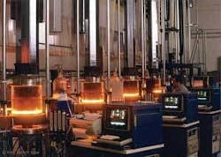
Producing crystalline silicon in crucibles schott solar / epiaAnother reason for the limited momentum during the first half century of PV's existence was the absence of a few dominant players defining the way forward for solar PV. By contrast, in the semiconductor market, companies such as IBM, Intel, Motorola and TI pushed forward cost reductions along Moore's path, focusing the entire research community on a common objective. After some time, important new players joined the effort, but the main targets were never discussed. In PV however there were many options, and no single winning technology has emerged. Both bulk silicon (mono or polysilicon) as well as thin film have compelling reasons for further investment in their research. And as if these options weren't enough, more new technologies have been explored in the last 10 years, and flexible thin film cells on polymer substrate, or multi-layered high efficiency cells, are getting closer to commercialization.
Though PV roadmaps exist, they are significantly less detailed than the ITRS roadmap, and they are all slightly different depending on the source. However, all the roadmaps agree on one thing: in order to make the PV industry viable in the long run, the price of electricity per energy unit (cost/kWp) generated by a photovoltaic system needs to be comparable with the electricity market price during daytime, or peak time. That cost target is 20 eurocents/kWp. In order to achieve this, significant efficiency improvements are needed in the production process, as well as in balance-of-system costs such as rectifiers and installation. Further in this article we will concentrate on where the semiconductor industry has seen opportunities to get involved.
The bulk of mainstream PV production is silicon based
Over the years the semiconductor industry has gathered an incredible amount of know-how about silicon in its different forms, such as monocrystalline and multi (poly)-crystalline silicon, amorphous silicon and thin-film silicon. Also silicon's interaction with other materials, such as aluminum and copper, is well understood. Such knowledge is very useful in the analysis of the behaviour of silicon-based solar cells, and in optimizing their efficiencies. For instance, the team of Dr Jef Poortmans, Programme Director for photovoltaics at IMEC, Belgium, is using the know-how that exists at IMEC from advanced deep-submicron research for its own research on thin-film PV cells on inexpensive substrate material such as metallurgical grade silicon or ceramics: 'Our understanding of epitaxial growth of silicon and the interactions with the substrate, has enabled us to grow large silicon crystals on low-cost substrate. This is the perfect material to make efficient PV cells at a significant lower cost', Dr Poortmans explained.
Equipment manufacturers, too, are using their experience from the semiconductor industry as a basis for their entry in the PV market. As growth rates are moving into the single digit area for semiconductors, the fast-growing PV market is regarded as a way of maintaining financial performance. However, entering the PV sector does not offer a 'free lunch', because major research is needed to adapt to the manufacturing needs of photovoltaics. In the past, microelectronics has been a batch-based process. This means that a set of a few (up to 30) wafers were processed for one set of parameters, and they were kept together in a box (also called a 'pod' or 'carrier') and moved from one piece of equipment or equipment chain to the other in that box. Batch processing of this type allows the device manufacturer to process different devices in the same production line, keeping the setup time to a minimum.
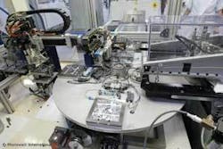
In PV manufacturing, however, maximizing throughput at a predefined process quality is the main objective. Batch processes are inherently less efficient than continuous systems because of the queuing of batches between the process steps. Thus one of the most important changes that equipment manufacturers have to implement in order to get their product accepted in the PV market is to rethink their material flow through the equipment to convert it to a continuous process. This is especially difficult for vacuum process steps, like PVD (physical vapour deposition). Companies such as Von Ardenne, Applied Materials (formerly Applied Films), Oerlikon and others are mastering these techniques, which are also applied for coating of architectural glass and flat panel displays (FPD).
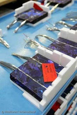
Many solar cell manufacturers have introduced their own standards. Industry wide norms would aid greater integration photowatt / epia
Another reason for the move of several semiconductor industries into photovoltaics is their observation that the PV industry still offers scope for the introduction of many of those process optimizations that have brought the semiconductor industry to its current level of efficiency. Examples include thorough standardization of the interfaces between different types of equipment, of the material characteristics of the consumables used in the production process, and last but not least of the automation interfaces to integrate the production and metrology equipment seamlessly in the advanced process control (APC) system (see boxed text below).
A further element is the advantage of scale: commodity semiconductor products are all made in a limited number of production facilities (fabs) that often make devices for many original equipment manufacturers (OEM). Together, Tower, Samsung, Matsushita, TSMC and UMC have close to 70% of this market. Only a few OEMs have sufficient volumes to maintain their own facilities - such as Intel, AMD, TI, Matsushita and others. This trend will also occur in PV, where we now see more players with production capacities approaching 1 GW/year. However, as long as the rate of growth continues as it is doing today, there will be sufficient opportunities within the market for small and large manufacturers to co-exist in the same market segment. Thus a consolidation of current players will take place in the next 5-7 years if there are no significant market changes. In the more distant future, however, we can expect to see market consolidation in several parts of the value chain of the PV industry, as in the semiconductor industry, where a few players will produce the bulk of the commodity solar cells, while smaller players will migrate to specialized niche products.
Cell production must continue to increase to meet soaring demand photowatt / epia
What are the main production improvements needed in PV manufacturing in the coming few years? First of all, there is still scope to decrease the thickness of wafers. However, there are some limiting factors, such as the bending and breaking of cells during manufacturing, and the recombination of electrons that migrate through the cell to the contacts at the back. Reducing the thickness of cells will have an impact on the output of the PV industry, as Dr Robert Gattereder of M+W Zander explained at the SEMI CIS Photovoltaic conference in October 2006 in Moscow: 'if the industry can reduce the use of silicon for crystalline silicon cells by 30%, by going from 10.5 g/W to 7 g/W, it would mean that the PV industry can produce 8.5 GWp/year instead of 5.6 GW/year from the same amount of feedstock. Another improvement that the industry is looking at is the increase of throughput by increasing cell size and processing speed, while keeping an acceptable yield. As a third item, processes need to improve to increase the average efficiency of the crystalline silicon cells from 15%-20% for monocrystalline silicon and from 16%-22% for Czochralski silicon.'
What can PV pass on?
The semiconductor industry has much to offer PV manufacturing; but can the semiconductor industry also learn from the PV industry? Yes! Several new techniques that were developed for the PV industry, such as wire sawing, can also be used within the semiconductor industry. At non-technical levels, too, the communities can learn from each other. Due to the dominance of the ITRS roadmap there were never sufficient resources to look into interesting alternative technologies, such as, for example, alternative memories (spin-tronics, or organic memories).
Since the physical limitations of silicon will bring the possibilities available under Moore's Law to a stop in 10-15 years, people are starting to look towards new options that will extend the possibilities of microelectronics. 'More than Moore' is the joined nominator for this trend, unifying technologies such as MEMS and nano with the digital logic and memories of the current electronic applications.
Yet there are so many possible options that the industry finds it difficult to start investing in 'More than Moore'. Organizations such as ENIAC (European Nanoelectronics Initiative Advisory Council) are trying to align the views on research in this area, and the RSC (Royal Society of Chemistry) is aligning industry needs and research opportunities. The PV industry can show the semiconductor industry how its research community has always worked closely together with industry, through technology transfers or spin-offs of research know-how.
Combined strengths
In many ways the semiconductor industry is a natural partner of the photovoltaic industry, and that both industries can benefit from the other through collaboration, in order to achieve the PV industry's challenging target - generating power at the same cost as conventional energy sources. The semiconductor industry can reduce its cyclic market effects and create new products in a growth market, in order to become again the darling of the financial world.
Eddy Blokken is Director, Technology and Standards, at SEMI Europe. SEMI is the global industry association for the semiconductor sector.
e-mail: [email protected]
web: www.semi.org
Notes
- First photovoltaic effects were detected in the early 19th century (1838), but the use of a p-n junction for solar cells was patented by Dr Ohl of Bell Labs.
- A technology node is a set of processes that can make integrated circuits (ICs) that have a certain minimal feature size. State of the art today is 60 nm minimal feature size, and first announcements of 45 nm are done (to put these dimensions in perspective: 45 nm relates to 1 metre, as 2 metres relates to the perimeter of the earth!). Technology nodes are defined industry-wide and agreed upon in the ITRS roadmaps.
Standards in PV
PV installations have to comply with national/international standards for (electrical) safety and compliance, environmental standards and other end-user specifications. A significant effort is being made on this type of topic by the International Electrotechnical Commission (EIC), partly in association with the PV GAP programme. Because several of the larger PV cell manufacturers are vertically integrated, they have developed their own in-house standards. If they were to decide to buy equipment from a third party, that equipment provider would need to adopt its equipment to the aforementioned company standard.
More and more new players in the PV industry are looking for third party equipment in order to build a complete production line. This trend can only be successful if industry standards are agreed upon for the interfaces that are used by these systems. This can be in the form of simple agreements - such as for the height and other dimensions of the input and output for a continuous flow system - or more sophisticated interfaces, such as machine-to-machine interfaces and their related software protocols for the advanced process control of the full production line.
Advanced Process Control
Advanced Process Control (APC) is a domain in the semiconductor business that has enabled the industry to shift rapidly from one technology node to another, while getting acceptable yields and predictable performance.2 It enables measurement of critical process parameters, directly or indirectly, with minimal interference to the process throughput. The next step is to analyse these hundreds of measurement points, which generate massive amounts of data both for the process steps, and also for the global process. Finally, the process parameters are adjusted slightly to optimize the yield of the products being manufactured, and the data can even be used to adjust the 'recipe' for the whole process. Such control is possible in the semiconductor business because standard interfaces have been agreed across the industry.
In PV manufacturing, however, there are not yet many types of equipment with the standardized machine-to-machine interfaces that would allow such yield improvements. Some companies have their proprietary APC system and interfaces, so for a manufacturer this will inhibit any change to other equipment vendors that not have that specific proprietary interface. The advantage of course is the one-stop-shop for all process related problems, reducing significantly the risks of building a new process line.
Recent industry trends
Applied Materials and Applied Films
In early September, Applied Materials, a dominant player in semiconductor equipment manufacturing for process equipment, announced its plans regarding PV. The first step was its acquisition of Applied Films, an expert in PVD systems for the deposition of thin coatings on different substrates. This technology is used to coat architectural glass with heat-reflecting films, but also for the creation of thin-film PV systems. Analysts commented on this move extensively, because it was an important step for Applied Materials, as well as for the wider PV industry. It assured Applied Materials' presence in a fast-growing market. While it didn't have an impact on the short-term results of Applied Materials, due to the complementary nature of both companies, and the similarity between the semiconductor and the PV industry, all analysts agreed that it was a logical move. For the PV industry the acquisition was an important signal that dominant players in a US$33 billion industry were getting involved in an industry that is much smaller today ($1 billion), but has significant potential in the future.
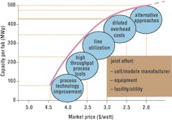
Figure 1. Optimum size of a PV production facility in relation to the cost/Wp. Source: M+W Zander, presented at SEMI CIS Photovoltaic conference, Moscow, 2006
Size matters
In 2005 only one PV cell manufacturer had more than 400 MW/year production capacity - Sharp (428 MW/year), with 25% market share. Second was Q-Cells, leaping from 4th to 2nd place, with 160 MW/year. Q-Cells expects to cross the 400 MW/year threshold in 2007, as do Kyocera and Sanyo. At the SEMI CIS Photovoltaic conference in October 2006 in Moscow, Dr Robert Gattereder of M+W Zander gave his view on the optimum size of a PV production facility, in relation to the cost/Wp. Taking into account the efficiency improvements that can be made in relation to overhead and yield reduction and the increase of throughput, Gattereder estimated that economic viable cells could be being manufactured in 500 MW facilities within 2-4 years.
Centrotherm
Centrotherm has been developing thermal treatment equipment for the semiconductor industry since 1976. Due to the explosive growth of PV in Germany and the Asian market, the company saw its main market shift from semiconductors to PV. This change forced it to rethink its organizational structure, and it created focused companies for semiconductor, PV and waste treatment.
Cypress and SunPower
SunPower, a spin-off from Stanford University, was founded by Dr Richard Swanson in 1988. The company developed one of the most efficient solar cells in mass production, with the help of Cypress Semiconductor, which invested in the company in 2002.
Feedstock
Until a few years ago the need for silicon was mainly dominated by the semiconductor industry. The industry agreed on long-term capacity forecasts with providers of purified silicon (feedstock). The PV industry was able to find sufficient material for its needs on the spot-market, using the temporary excesses of semiconductor silicon. However, since 2005 demand for silicon has increased significantly in the PV-industry, even overtaking the capacity needs of the semiconductor industry. This has resulted in high prices for silicon on the spot-market, forcing PV production facilities to work at less than full capacity. In order to avoid this, the PV industry saw the need to agree on long-term capacity forecasts, so it would be able to secure the raw material for their production lines. Because it takes about 2 years to build these additional capacities, it will take still to 2008 and beyond before silicon prices will go back to normal, between US$30-40/kg for solar-grade silicon. An additional advantage of this evolution is that more solar-grade production will become available, which will be cheaper than the semiconductor grade silicon, because material characteristics towards purity are less stringent for the PV industry.
Another interesting development is the use of alternative, less expensive, techniques to create solar grade silicon (SoG-Si). Recently two independent sources claimed that they are commercializing a chemical purification method that will be significantly less expensive than the classical methods. Dow Corning has announced that it is offering SoG-Si to its customers that was derived from metallurgical poly-silicon feedstock. As production costs can be lower for this process, it offers opportunities to lower the overall cost of the PV cell, assuming enough can be produced.
