Laser pump-probe imager sorts semiconductor and metallic nanotubes
West Lafayette, IN--Researchers at Purdue University have created an imaging tool that rapidly screens single-walled carbon nanotubes (SWNTs), sorting them into their semiconducting and metallic versions.1
While semiconducting SWNTs could one day replace the semiconductors in conventional components and circuits (making them smaller and faster), metallic SWNTs can't. But when semiconducting SWNTs are fabricated, the metallic versions unavoidably form too, contaminating the semiconducting SWNTs.
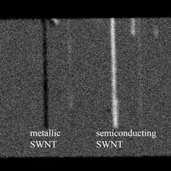
However, the new imaging tool could solve this problem, says Ji-Xin Cheng of Purdue, one of the researchers. In the tool, a pulsed pump laser excites the SWNTs from a ground state to an excited state; a probe laser then reveals which types of SWNTs are which.
The technique, called transient absorption, measures the "metallicity" of the tubes. The detection method could be combined with another laser to destroy the unwanted metallic nanotubes as they roll off of the manufacturing line, leaving only the semiconducting tubes.
The nanotubes have a diameter of about 1 nm, making them far too small to be seen with a conventional light microscope. "They can be seen with an atomic-force microscope, but this only tells you the morphology and surface features, not the metallic state of the nanotube," Cheng said.
Label-free sorting
The transient-absorption imaging technique represents the only rapid method for telling the difference between the two types of nanotubes. The technique is "label-free," meaning it does not require that the nanotubes be marked with dyes, making it potentially practical for manufacturing, said Cheng.
The researchers performed the technique with nanotubes placed on a glass surface. Future work will focus on performing the imaging when nanotubes are on a silicon surface to determine how well it would work in industrial applications.
"We have begun this work on a silicon substrate, and preliminary results are very good," Cheng said.
Future research also may focus on how electrons travel inside individual nanotubes.
REFERENCE:
1. Yookyung Jung et al., Phys. Rev. Lett. 105, p. 217401 (2010).
Subscribe now to Laser Focus World magazine; it’s free!
About the Author

John Wallace
Senior Technical Editor (1998-2022)
John Wallace was with Laser Focus World for nearly 25 years, retiring in late June 2022. He obtained a bachelor's degree in mechanical engineering and physics at Rutgers University and a master's in optical engineering at the University of Rochester. Before becoming an editor, John worked as an engineer at RCA, Exxon, Eastman Kodak, and GCA Corporation.