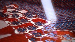
Self-assembled optical metasurface sensors for bioscience are dielectric, not metallic
Engineers from École polytechnique fédérale de Lausanne (EPFL Lausanne, Switzerland) have now discovered a simple way of creating optical metasurfaces in just a few minutes—without needing a clean room and using a simple "dewetting" method.1 The metasurfaces could be used to create flexible sensors to be placed directly on a patient's skin to measure things like pulse and blood pressure, or to detect specific chemical compounds.
Creating metasurfaces using conventional photolithographic methods, is a fastidious, several-hour-long process that must be done in a clean room. But the EPFL group has now developed a simple method for making them in just a few minutes, resulting in dielectric glass metasurfaces that can be either rigid or flexible. The new method exploits a natural process already used in fluid mechanics: dewetting. This occurs when a thin film of material is deposited on a substrate and then heated. The heat causes the film to retract and break apart into nanoparticles.
"Dewetting is seen as a problem in manufacturing, but we decided to use it to our advantage," says Fabien Sorin, one of the researchers. Using this approach, the engineers were able to create dielectric glass metasurfaces (as opposed to the usual metallic metasurfaces) for the first time.
The advantage of dielectric metasurfaces is that they absorb very little light and have a high refractive index. To construct these metasurfaces, the engineers first created a substrate textured with the desired architecture. Then they deposited chalcogenide glass in films tens of nanometers thick. The substrate was subsequently heated for a couple of minutes until the glass became more fluid and nanoparticles began to form in the sizes and positions dictated by the substrate's texture. The engineers' method is so efficient that it can produce highly sophisticated metasurfaces with several levels of nanoparticles or with arrays of nanoparticles spaced just 10 nm apart. That makes the metasurfaces highly sensitive to changes in ambient conditions, such as the presence of even very low concentrations of bioparticles.
Source: https://actu.epfl.ch/news/next-generation-optics-in-just-two-minutes-of-cook
REFERENCE:
1. Tapajyoti Das Gupta et al., Nature Nanotechnology (2019); https://doi.org/10.1038/s41565-019-0362-9.
About the Author
John Wallace
Senior Technical Editor (1998-2022)
John Wallace was with Laser Focus World for nearly 25 years, retiring in late June 2022. He obtained a bachelor's degree in mechanical engineering and physics at Rutgers University and a master's in optical engineering at the University of Rochester. Before becoming an editor, John worked as an engineer at RCA, Exxon, Eastman Kodak, and GCA Corporation.

