One of humankind’s core attributes is its tendency to push boundaries. From innovations in the arts and sciences to the pushing of actual territorial borders, we sometimes seem incapable of being satisfied with things the way they are. When we strive against each other, we get politics (and sometimes worse); when we strive against the limits of knowledge, we get Nobel Prizes.
In science and engineering, the limits we struggle to move beyond can be roughly and perhaps arbitrarily divided into the large, the small, and the in-between. As for the large and small: since Edwin Hubble’s discovery of the galactic redshift, we’ve managed to expand our concept of the universe to 93 billion light years in size, while atomic-force and scanning-tunneling microscopes have allowed us to visualize not just atoms, but their atomic orbitals as well. The National Ignition Facility’s lasers have produced temperatures to 100 million K, while scientists at the Massachusetts Institute of Technology (MIT; Cambridge, MA) have managed to cool a gas to less than 1 nanokelvin–a few billion times closer to absolute zero than the cold of interstellar space.
Much innovation lies in the in-between, however, such as the discovery of electromagnetic induction by Michael Faraday, which led to the development of electric motors and generators; and the invention by Joseph Fourier in the 1800s of the mathematical transform that bears his name, and that aids in the modern understanding of optical imaging and many other physical processes.
The discipline of photonics certainly produced its share of discoveries and new devices this year. And while the innovations came in all shapes and sizes, there’s no better place to begin than at the extremes.
From yocto to exa
Made small enough, a laser can fit in a photonic circuit or on a miniature probe–often, the smaller the laser, the better. But traditionally, a laser cavity must be at least half as long as the wavelength of light it produces. However, thanks to plasmonics, that limit no longer applies. This year, researchers at Norfolk State University (Norfolk, VA), Purdue University (Purdue, IN), and Cornell University (Ithaca, NY) created a 44-nm-diameter laser–or, more accurately, a “spaser” (surface plasmon amplification by stimulated emission of radiation)–that, when optically pumped, produces resonating surface plasmons in its 14 nm gold core. Outcoupling of the resonance produces 531 nm light. And scientists at the University of California at Berkeley announced a laser in which lasing occurs in a cadmium sulfide nanowire with a silver surface separated by an insulating gap of just 5 nm. Also optically pumped and depending on surface plasmons, the device emits at 489 nm.
If made large, precise, and energetic enough, a laser–at least if it’s a free-electron laser (FEL)–can be made to emit x-rays. This is just what was accomplished at the SLAC National Accelerator Laboratory (Stanford, CA), where the Linac Coherent Light Source (LCLS) now emits 80 fs pulses of light tunable between 0.15 and 1.5 nm. In a FEL, an electron beam passes through a magnetic “undulator” that causes the electrons to oscillate laterally as they pass through. While high powers in the IR have been obtained from FELs for years, producing x-rays requires incredibly precise undulator construction and very high electron energies, both achieved at SLAC. Uses of the LCLS include recording holograms of individual protein molecules.
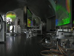
Research based on light at petawatt (1015 W) levels is now possible with high-peak-power ultrafast laser systems in operation at the University of Texas at Austin, the Rutherford Appleton Laboratory (Didcot, England), Osaka University (Osaka, Japan), and the Laboratory for Laser Energetics (Rochester, NY). For example, nuclear-fusion studies are being carried out at the University of Texas using its Texas Petawatt laser, with the resulting neutrons being used for materials-science studies (see Fig. 1). However, petawatt power levels are by no means the limit.
Todd Ditmire, project director of the Texas Petawatt laser, says that the device, which has the highest peak power of any laser system now operating, has the potential to reach the exawatt (1018 W) level. The laser currently produces 190 J, 100 fs pulses; by using new laser glass materials and a high-gain chain of amplifiers, it could be made to produce 100 kJ pulses and exawatt peak powers, which would perhaps result in power densities of up to 1025 W/cm2 (the Texas Petawatt currently can produce a 1021 W/cm2 power density).
The advent of attosecond (1 as = 10-18 s)-scale laser light pulses has opened up new approaches to atomic and nuclear physics. But attosecond physics is possible using longer light pulses. Ursula Keller and others at the Institute for Quantum Electronics at the Swiss Federal Institute of Technology (ETH Zurich, Switzerland) created what they call an “attoclock” and used it to measure a 12-attosecond upper limit on the tunneling delay time (the time it takes an electron to escape the binding potential of an atom before the atom becomes ionized) for the strong-field ionization of a helium atom. In a technique called attosecond angular streaking, the electric field of an almost circularly polarized 725 nm femtosecond pulse from a Ti:sapphire laser focused on the helium rotates 360° in space every 2.4 fs, as if it were a clock’s hand; a detector measures the direction of the ionized electron as it leaves the helium, pinpointing the time of the event to attosecond accuracy.
But attosecond photonics may soon be passé. Andreas Ipp and his colleagues at the Max Planck Institute for Nuclear Physics (Heidelberg, Germany) recently laid the theoretical groundwork for the production of light pulses a million times shorter–in the yoctosecond (10-24 s) range. Under the right conditions, a quark-gluon plasma (QGP)–produced by the high-energy collision of heavy ions–could produce a gamma-ray pulse, or possibly even two pulses that could be used for pump-probe experiments. Such high-energy photons have already been detected from QGPs, although pulse durations have not yet been measured.
Optics: always a bright spot
While one of this year’s greatest achievements in optics—the upgrading of the Hubble telescope—was highly publicized in the general media, many interesting advances were made known mainly in technical journals.
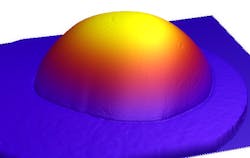
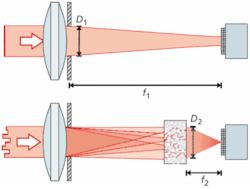
For example, a tunable fluidic lens developed by researchers at the Fraunhofer Institut Angewandte Festkörperphysik (Freiburg, Germany) is made of a chamber with variable fluid volume, sealed by a flexible transparent membrane; however, rather than the usual polymer or silicone membrane, this lens is contained by a flexible diamond film.1 A nanocrystalline diamond membrane 150 nm thick was grown on a silicon (Si) wafer and a hole ranging from 1.3 to 2.5 mm etched through the Si to create a chamber. When filled with microscope-immersion oil (n = 1.46) and the pressure varied, a 2.5-mm-diameter lens was adjusted in focal length from infinity to 7.5 mm, while a 1.3-mm-diameter lens was tuned from infinity to 3.5 mm in focal length (see Fig. 2). The lenses are impermeable to gases, chemically stable, and transmit from 20% at 200 nm to 80% at 700 nm (limited by interference effects). Potentially mass-producible, such lenses could be useful in cell phones and other digital devices.The resulting spot is much smaller than the original diffraction limit (which is possible because the scatterer results in a higher numerical aperture); more important, the spot is always the exact theoretical lower limit in size. Experimental limitations on the SLM do not affect the spot size; they only increase the amount of background scattered light. The researchers note that disordered scattering has previously been used to improve resolution with ultrasound, radio, and microwaves, and may be used in the future to achieve superresolution with disordered plasmonic nanostructures.
As for the intrusion of plasmonics into ordinary bulk optics, scientists at Academia Sinica (Taipei, Taiwan), National Tsing-Hua University (Hsinchu, Taiwan), National Taiwan Ocean University (Keelung, Taiwan), and National Yang-Ming University (Taipei, Taiwan) are hoping to make it so by developing plasmonic nanoslit arrays that can replace traditional waveplates for some purposes.3 The group fabricated arrays with a 500 nm period and slit widths ranging from 100 to 500 nm, created from 150-nm-thick layers of gold (they also tried nickel but it didn’t work). Although narrower slits transmitted less light, they were also more birefringent: at 632.8 nm, the 300-nm-slit arrays had a birefringence (refractive-index difference between orthogonal polarizations) of about 1, while the 100-nm-slit arrays reached a birefringence of 2.7. The researchers created quarter- and half-wave plates, and note that the devices can be simply made using nanoimprint lithography.
Transformation optics—that seemingly magical area of invisibility cloaking and optical black holes—still remains mostly theory, but researchers have experimentally cloaked an object in broadband light, although the object is merely a bump in a mirror. And, based on ideas from Tomas Tyc from Masaryk University (Brno, Czech Republic) and Ulf Leonhardt from the University of St. Andrews (St. Andrews, Scotland), Ma Yun Gui, and Ong Chong Kim of the National University of Singapore built a perfect retroreflector for microwave radiation. Translating the retroreflector from the microwave to the visible-light range would mean giving up straightforward macroscopic construction and delving into the much-more-involved micro- and nanostructure fabrication used for optical metamaterials.
As for practicality, a new type of contact lens developed by researchers at Xceed Imaging (Petach-Tikva, Israel), Tel Aviv University (Tel Hashomer, Israel), and Bar-Ilan University (Ramat-Gan, Israel) creates an extended depth of focus with the addition of a few concentric annular rings of less than 1 µm in depth on the front surface of the lens. The rings create phase shifts that cause constructive interference around the focal plane and destructive interference elsewhere. The resulting three-diopter extended depth of field comes with a small loss in contrast that is compensated for by the human brain; people with astigmatism benefit especially from the improved lenses.
A fiber for every purpose
Optical fibers are finding ever-expanding uses. A group at Femtolasers Produktions (Vienna, Austria) has developed ways to deliver ultrafast (24 fs) laser pulses through fiber lengths of up to a couple of meters.4 Fiber delivery allows radiation to be delivered to moving or awkward-to-reach targets, but fiber dispersion and optical nonlinearity make ultrafast pulses difficult to transmit over fiber. The Femtolasers group begins with pulses at 792 nm with a 48 nm bandwidth, combining dispersive mirrors with either prism or grating compressors in the pre-fiber optics. No dispersion-correction optics are required after the fiber. Pulses with a 1 nJ energy were delivered through a 1.6 m length of large-mode-area (17 µm) fiber–the shortest pulses ever delivered through a single-mode fiber with a length of more than 1 m, according to the researchers.
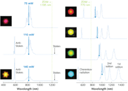
Conversely, as is well known, nonlinearities in a microstructured (or even conventional) fiber can be exploited to create a white-light supercontinuum from ultrafast IR pulses by matching the fiber’s zero-dispersion wavelength (ZDW) with that of the pulses. However, as Haohua Tu and Stephen Boppart at the University of Illinois at Urbana-Champaign (Urbana, IL) have discovered, by detuning the ZDW far away from the laser wavelength to create a “short nonlinear-interaction condition,” the laser pulse energy can be switched into a different, isolated spectral band, which can be chosen to be anywhere in the visible range (see Fig. 4). The result is a versatile ultrafast source with a relatively high average power within a small visible spectral band (see laserfocusworld.com/articles/365412).As for fiber-based sensors, one way to increase the interaction of light within an unclad optical fiber with its surrounding environment is to create a smaller-diameter “waist” in the fiber; this increases the influence of evanescent waves, which exist at the fiber’s surface and extend (with an exponentially decaying intensity) into the surrounding medium. However, the result is a very delicate section of fiber at most a few microns in diameter that can be easily contaminated with dust. Researchers at the University of Bath (Bath, England) and the University of Sydney (Sydney, Australia) avoid this problem by embedding the fiber and its waist in an aerogel. Gas-permeable and with a refractive index close to that of air, but with a structure rigid enough to hold a fiber in place and allow normal handling, the aerogel lets surrounding substances interact with the evanescent field and also keeps contaminating particles away. Fibers with waists down to 1 µm in diameter were formed into aerogel-based sensors.
With the growth of fiber to the home, ordinary communications optical fiber is becoming more highly developed–not just in its carrying capacity, but in its practicality. Bend-insensitive fibers (BIFs) are finding increasing use, driving researchers to push the limits of their performance. For example, a group at the Gwangju Institute of Science and Technology (GIST; Gwangju, South Korea) has created a BIF with a record-low bending loss of 0.014 dB per loop at 1550 nm for a loop of 5 mm radius; if put in use, such a fiber would be just that much easier to route into and around a home (just think–it could be wound tightly around your finger 100 times and lose only 1.4 dB of its signal).
The GIST-developed single-mode fiber combines mode-field-diameter optimization (in which the core refractive-index profile is optimized to keep the mode away from the cladding) with low-index trenching (which consists of a narrow radially symmetric region in the cladding that has a lowered refractive index). The experimental fiber was fabricated with a modified chemical-vapor-deposition technique that could leave some unpredictability in the core refractive-index profile, so the researchers assumed the worst case–that the center of the core would reach an index as low as the cladding–so that they would not have to depend on expensive manipulations of the fiber preform to reach their goals. The resulting fiber can be spliced to ordinary single-mode fiber with a maximum splicing loss of 0.467 dB at 1550 nm.
Capturing photons
A photon detector invented by scientists from the Bio-Inspired Sensors and Optoelectronics Laboratory at Northwestern University (Evanston, IL) avoids the usual semiconductor configuration and instead can be called optoelectromechanical.5? Comprising a nanoscale tip on a cantilever, it is identical to an atomic-force-microscope probe, except that the electric field and charge focused by the tip is influenced by incoming light. The change in electrostatic force moves the tip, and the movement is monitored. The researchers theoretically modeled the vibrating detector tip, even including the exotic Casimir force in the model (sometimes called “the force from nothing,” the Casimir force arises when two conducting objects are close enough together to affect the so-called “virtual photons” between them that arise through quantum electrodynamics. The force is usually evident only for nanometer-scale gaps.)
Experimental results for the nanotip detector in the shortwave IR range show a responsivity of 276 A/W–equivalent to 220 electrons per incoming photon–and a room-temperature noise-equivalent power of 3.53 × 10⁻¹⁴ W/Hz1/2. The researchers believe that custom versions of the detector could approach the theoretical limit of detecting single photons at room temperature.
Another mechanically based detector, this one for terahertz radiation, has been created by researchers at the Clausthal University of Technology (Goslar, Germany), the Laboratorio NEST (Pisa, Italy), and the University of Cambridge (Cambridge, England). The room-temperature device is built around a miniature quartz tuning fork from a standard wristwatch; radiation modulated at the tuning fork’s 32 kHz natural frequency causes the tuning fork to vibrate as a result of radiation pressure. The vibration is sensed by measuring the fork’s piezoelectric current.
The combination of germanium (Ge) and Si for detectors is an excellent one for more than one reason, as researchers at Intel Corporation well know (Santa Clara, CA). This year Intel, along with researchers at the University of California–Santa Barbara, the University of Virginia (Charlottesville, VA), and Chemin de Crey-Derrey (Châtel-St-Denis, Switzerland) fabricated a GE/Si avalanche photodiode (APD) with an enhanced gain-bandwidth product of 845 GHz at a 1310 nm wavelength (standard III-V APDs can reach only about 120 GHz).6 With a gain of 65 and a bandwidth of 13 GHz at a -30 dBm optical input, the Ge/Si detector relies on the high absorption of Ge at that wavelength and the good performance of Si as a multiplication layer. The fabrication process is CMOS-compatible, which Intel is surely thrilled about. Waveguide-based Ge/Si APDs could be next, says Intel.
The record efficiency for a photovoltaic solar cell today hovers at just above 40%, with all contenders for the title being multijunction cells. Rather than monolithically growing the junctions atop each other, IMEC (Leuven, Belgium) is mechanically stacking them. A Ge and a gallium arsenide layer have already been combined; a triple-junction cell (with the third layer being indium gallium phosphide) should be working by the beginning of 2010, says IMEC. Perhaps more important due to its potentially much lower cost is a prototype for a hybrid cell developed by RoseStreet Labs Energy (RSLE; Phoenix, AZ). Combining an economical nitride thin film with Si and its large manufacturing infrastructure, the cell should have an efficiency of 25% to 30% and could be in production by the end of 2010.
Seeing things
As always, flat-panel displays are undergoing intense development, especially thinner, lighter displays. Engineers at Universal Display (Ewing, NJ) are creating full-color organic LED (OLED) displays on metal-foil substrates that can be repetitively flexed–for example, being rolled 2500 times around a one-inch cylinder–without failure. A prototype QVGA (320 × 240 pixel) display has an amorphous-Si backplane on 76-µm-thick steel foil with a resolution of 100 pixels per inch and an OLED layer thickness between 100 and 200 nm. The phosphorescent OLED material system can have internal quantum efficiencies of up to 100%.
Unlike most reflective displays (meaning those that do not provide an illuminated image, but instead have pixels that simply change reflectivity to produce an image), a lithographically fabricated electrofluidic display created by researchers at the University of Cincinnati and Sun Chemical (both in Cincinnati, OH) has visually brilliant color pigments, reaches a reflectivity value of 55%, and can potentially reach an 85% reflectivity. Small pigment reservoirs span less than 10% of the pixel area; a voltage across two electrowetting plates can draw the pigment from the reservoir and spread it across the normally mirrorlike aluminum pixel. The same technology could be used for tunable-color cell-phone cases or adaptive camouflage, say the researchers.
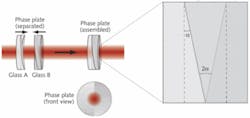
Stimulated emission-depletion (STED) microscopy has become a very effective way to image biological cellular features with a resolution better than that of confocal microscopy. In STED microscopy, the focal spot of the scanned excitation beam is superimposed with the ring-shaped focus of a second laser beam that blocks fluorescence from occurring anywhere except the very small dark center of the ring. But because they require precise alignment of two beams, STED microscopes are complicated things. However, a group at the Max Planck Institute for Biophysical Chemistry (Göttingen, Germany) has invented an optical element that, when used in a STED system, eliminates one beam path and aligns the central and ring-shaped foci by design.
Both beams pass through a single-mode fiber (automatically keeping them aligned), but it is the design of the additional optical element, a dual-wedge phase plate, that is the core of the STED system. Two identical cemented pairs of wedges, each made of two different glasses, are placed in the element so that, looking from the side, the wedges are at opposite orientations (see Fig. 5). At one laser wavelength (that of the central spot), the glasses have identical refractive indices, and thus do not affect the diffraction-limited spot. At the other laser wavelength (that of the ring), the glasses have differing indices; thus, the wedges form a vortex phase plate that produces a ring-shaped focus. Radically simplifying such a complex imaging instrument using such an ingenious approach is a true achievement.Zap
The inventiveness of those in the photonics community knows no bounds. As a result, a true compilation of this past year’s achievements, including applications, would require the efforts of many people diligently creating a Wikipedia-type database. Please peruse our own photonic fence” that will kill mosquitoes, but not other insects, using a laser. Imaged by a CMOS sensor and distinguished by their wingbeat frequency, the mosquitoes will then be killed by a laser (with specific properties that are, as if it were a military laser, being kept secret). The fact that Intellectual Ventures is located in the same city as a major office of Microsoft may be a coincidence–but it turns out that, with its potential to reduce malaria, Kare’s project is being funded by Bill Gates (as well as the United Nations).
REFERENCES
- A. Kriele et al., Appl. Phys. Lett. 95, p. 031905 (2009).
- I. M. Vellekoop et al., arXiv:0910.0873v1 [physics.optics] (5 Oct 2009).
- Shen-Yu Hsu et al., Appl. Phys. Lett. 95, p. 013105 (2009).
- Tuan Le et al., Optics Exp. 17, p. 1240 (Feb. 2, 2009).
- J. Kohoutek et al., Optics Exp. 17, p. 14458 (Aug. 17, 2009).
- W. Sfar Zaoui et al., Optics Exp. 17, p. 12642 (July 20, 2009).
About the Author
John Wallace
Senior Technical Editor (1998-2022)
John Wallace was with Laser Focus World for nearly 25 years, retiring in late June 2022. He obtained a bachelor's degree in mechanical engineering and physics at Rutgers University and a master's in optical engineering at the University of Rochester. Before becoming an editor, John worked as an engineer at RCA, Exxon, Eastman Kodak, and GCA Corporation.
