Sony unveils stacked structure for CMOS sensors
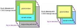
Tokyo, Japan--Sony Mobile Communications has developed miniature back-illuminated CMOS image sensors that contain pixels stacked over their electrical circuits rather than laid out beside them, saving space and improving the pixel percentage fill. The sensors, which are four to five millimeters square, come in 8 and 13 megapixel configurations.
The sensor series, dubbed "Exmore RS," has red-green-blue-white (RGBW) coding and a high-dynamic-range movie function. Sony says the RGBW coding function can capture sharp, clear images even when filmed or photographed in low-light conditions because it contains white pixels in addition to conventional RGB pixels.
The stacking technology will allow Sony to make smaller cameras for cellphones and other devices to help maximize space for larger screens. Sony will also bring to market three compact autofocus imaging modules equipped with autofocus and lens units optimized for the industry’s smallest 1.12 µm unit pixel size.
Sony says it is is committed to strengthening its production capacity for stacked CMOS image sensors. The company plans to invest in Sony Semiconductor Corporation's Nagasaki Technology Center in 2013 and 2014 to increase the production capacity for stacked CMOS image sensors. The investment will provide for new wafer-processing equipment for stacked CMOS image sensors, as well as increasing and transforming wafer lines capable of manufacturing CMOS image sensors. Sony plans to increase total production capacity for CCD and CMOS image sensors to approximately 60,000 wafers per month by the end of September 2013.
Sources: http://www.sony.net/SonyInfo/News/Press/201208/12-107E/index.html; http://www.sony.net/SonyInfo/News/Press/201206/12-084E/index.html
About the Author

John Wallace
Senior Technical Editor (1998-2022)
John Wallace was with Laser Focus World for nearly 25 years, retiring in late June 2022. He obtained a bachelor's degree in mechanical engineering and physics at Rutgers University and a master's in optical engineering at the University of Rochester. Before becoming an editor, John worked as an engineer at RCA, Exxon, Eastman Kodak, and GCA Corporation.