Laser-enabled advanced packaging assembles chips onto flex substrates
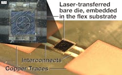
| A small die has been transferred and affixed to interconnects on a flex substrate using laser-enabled advanced packaging (LEAP). (Image: NDSU) |
Fargo, ND--North Dakota State University (NDSU) scientists have developed a laser-assisted technique for assembly of ultrathin semiconductor chips onto rigid and flexible substrates. Called laser-enabled advanced packaging (LEAP), the approach allows semiconductor chips less than 50 µm thick to be rapidly placed and fixed at specific locations and orientations with high precision.
The technology has the potential to enable high-volume handling, placement, and interconnection of miniature microelectronic components, including various types of active and passive embedded components. LEAP has been under development by the Advanced Electronics Packaging research group at the North Dakota State University Center for Nanoscale Science and Engineering (CNSE) since 2008.
Recently the NDSU researchers used technology to fabricate a functional electronic device with a laser-assembled, ultrathin silicon chip embedded in a flexible substrate. A key part of LEAP is a (patent-pending) process called thermo-mechanical selective laser-assisted die transfer (tmSLADT). “The LEAP technology and tmSLADT process are important because they potentially enable a new class of inexpensive electronic devices by the high-volume placement and interconnection of various types of ultra-thin, fine pitch, active and passive circuit components,” said Aaron Reinholz, associate director for electronics technology at NDSU CNSE. “These types of components are especially of interest for flex-substrate electronics, as they allow devices to bend, roll, and be manipulated into complex geometries.” Such devices include garment-integrated RFID tags, intelligent sensors platforms, and self-adapting conformal antennas.
The LEAP technology is outlined in “Laser-Enabled Advanced Packaging of Ultrathin Bare Dice in Flexible Substrates,” accepted for publication by IEEE Transactions on Components, Packaging and Manufacturing Technology, manuscript TCPMT-2011-105.
