Surrey NanoSystems sells new nanomaterial growth systems for optoelectronics and other uses
Newhaven, England--Surrey NanoSystems announced the first sales of its new nanomaterial growth system, the NanoGrowth-Catalyst, to the École Polytechnique of Montreal (Montreal, QC, Canada) and the University of Surrey's Advanced Technology Institute (ATI; Surrey, England).
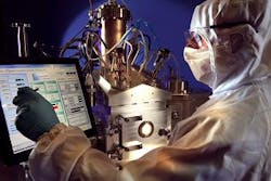
The NanoGrowth-Catalyst is a platform for work on nanomaterials including carbon nanotubes (CNTs), silicon nanowires, graphene, and nanoparticles for semiconductor and optical devices and other applications. The growth system's multichamber design ensures pure nanomaterial processing conditions by continuously maintaining the substrate under vacuum, from the deposition of catalysts to growth of materials.
The ATI is a partner to Surrey NanoSystems and has already been using an earlier version of the NanoGrowth system for around four years to support its research into next-generation semiconductor and photonic device technologies. ATI is the first customer to receive the new NanoGrowth-Catalyst. Facilities including a rapid infrared heating process and a water-cooled chuck are helping ATI to grow ordered CNT structures while maintaining the substrate below 350°C.1 Low temperature processing is critical as CNTs are conventionally grown at around 700°C—a level incompatible with CMOS semiconductor fabrication.
The other NanoGrowth-Catalyst system will be installed in Montreal, where it will support a wide range of research groups from the École Polytechnique and The University of Montreal studying topics including optoelectronics, microelectronics, and thin-film physics.
Surrey NanoSystems also built a third system for its in-house nanomaterials research, targeting materials for new forms of conducting via structures and dielectric materials to support the continued scaling of semiconductor devices. This system has three processing chambers and automated handling. Spare capacity on this tool will be made available to universities and their researchers working in related fields.
Surrey NanoSystems is represented in the USA by Axiom Resources Technologies (Placentia, CA).
REFERENCE:
1. Guan Yow Chen et al., "Growth of carbon nanotubes at temperatures compatible with integrated circuit technologies," Carbon, Vol. 49, Issue 1, p. 280, January 2011.
Subscribe now to Laser Focus World magazine; it’s free!
About the Author

John Wallace
Senior Technical Editor (1998-2022)
John Wallace was with Laser Focus World for nearly 25 years, retiring in late June 2022. He obtained a bachelor's degree in mechanical engineering and physics at Rutgers University and a master's in optical engineering at the University of Rochester. Before becoming an editor, John worked as an engineer at RCA, Exxon, Eastman Kodak, and GCA Corporation.