Highly flexible OLED light source has 10 micron bend radius
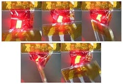
Tokyo, Japan and Linz, Austria--A group led by Takao Someya, professor at the School of Engineering at the University of Tokyo, has developed a thin-sheet organic LED (OLED) light source that functions even after being crumpled. The minimum bending radius and brightness of the sheet are 10 µm and 100cd/m2, respectively; the mass and thickness are 3g/m2 and 2 µm.
The same group also announced a thin-film pressure-sensor sheet that functions even after being crumpled and has a mass of only 3g/m2, which is about 1/27 that of ordinary paper. For the pressure-sensor sheet, it succeeded in forming an array of organic thin-film transistors (TFTs) that form an electronic circuit on the film substrate.
In 2011, the group developed a thin, light OLED photovoltaic (PV) cell that can be used as an optical sensor.
Three devices together can form medical sensor
These three devices (organic TFT as a component of an electronic circuit, optical sensor, and light-emitting device) together form all the elements necessary for medical and health-care sensors that can be integrated on a single ultrathin sheet.For collecting biological information such as the amount of oxygen in blood, devices made by combining a light source and light-sensitive detector are widely used. The research group expects that the new OLED light source will be used for medical and health-care wearable devices that use light as a probe to collect a variety of biological information.
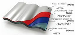
To directly form OLED elements on a 1.4-µm-thick plastic film substrate, which tends to be damaged in the manufacturing process, the group eliminated indium tin oxide (ITO) electrodes, which require a high-energy plasma film-forming process. Instead, it used a conductive polymer (PEDOT:PSS) that forms a film via a low-temperature, low-energy spin-coating process.
The group conducted the research in cooperation with researchers at Johannes Kepler University of Linz (Linz, Austria). The results were published on July 28, 2013 in the online version of Nature Photonics.
Sources:
http://techon.nikkeibp.co.jp/english/NEWS_EN/20130730/295194/
http://techon.nikkeibp.co.jp/english/NEWS_EN/20130726/294563/
About the Author
John Wallace
Senior Technical Editor (1998-2022)
John Wallace was with Laser Focus World for nearly 25 years, retiring in late June 2022. He obtained a bachelor's degree in mechanical engineering and physics at Rutgers University and a master's in optical engineering at the University of Rochester. Before becoming an editor, John worked as an engineer at RCA, Exxon, Eastman Kodak, and GCA Corporation.


