NIST carbon-nanotube-slit spectrometer collects climate data
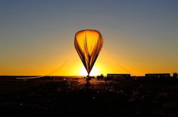
Boulder, CO--On September 29, 2013, a huge plastic balloon floated high in the skies over New Mexico carrying instruments to collect climate-related test data with the help of carbon nanotube chips made by the National Institute of Standards and Technology (NIST). The onboard instrument was an experimental spectrometer designed to collect and measure visible and infrared wavelengths of light ranging from 350 to 2300 nm. Simpler, lighter, and less expensive than conventional counterparts, the spectrometer was tested to determine how accurately it can measure the relative energy of light emitted by the Sun and subsequently reflected or scattered by the Earth and Moon.
The flight was launched from the Columbia Scientific Balloon Facility in Fort Sumner, NM. The balloon travelled with the wind in the stratosphere for about 8.5 hours before radio commands sent the payload parachuting back to Earth. The flight was the first of two intended to demonstrate experimental techniques and acquire sample measurements having possible future applications to Earth climate studies.
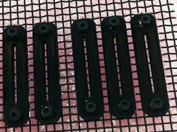
Researchers at NIST made the spectrometer's "slit," a high-precision chip that selected the entering light. The device was made under a recent agreement between NIST and the University of Colorado Boulder's Laboratory for Atmospheric and Space Physics (LASP). The slit was then calibrated at NIST's Gaithersburg, MD headquarters.
For nearly a decade, NIST Boulder researchers have been using carbon nanotubes, the darkest material on Earth, to make coatings for laser power detectors. Nanotubes efficiently absorb nearly all light across a broad span of wavelengths, a useful feature for reducing internal scatter in the balloon imager. NIST also has facilities for, and expertise in, pairing nanotubes with micromachined silicon chips.
For the balloon spectrometer, known as HySICS (HyperSpectral Imager for Climate Science), NIST made two types of custom chips that were stacked together in a sandwich. In the middle were aperture chips, coated with aluminum to block light transmission through the silicon, with small rectangular openings etched into the chip to allow light into the instrument. A precision spectrometer must ensure that it only gathers light coming directly from its target, so the two outer layers of the sandwich were masking chips—larger openings etched at an angle and coated with tall, thin carbon nanotubes. These VANTAs ("vertically aligned nanotube arrays") act as superefficient sponges to absorb scattered or stray light across the entire spectral range of the Sun.
While the balloon was in flight, the spectrometer scanned the slit across the Sun to measure solar irradiance. Spectral filters were calibrated by scanning the slit across the Moon and making measurements with and without filters in the beam path. The spectrometer also imaged light emitted from the Earth using the Sun as a reference light source.
NIST's experimental slit was made as part of the LASP Instrument Incubator Project, which fosters the development and evaluation of innovative remote-sensing concepts. LASP scientists will analyze data from the balloon flight in the coming months. For more about the balloon experiment, see http://lasp.colorado.edu/home/blog/2013/10/01/lasp-balloon-launches-with-first-of-its-kind-test-instrument/.
SOURCE: NIST; http://www.nist.gov/pml/div686/lasp-102213.cfm#
About the Author

Gail Overton
Senior Editor (2004-2020)
Gail has more than 30 years of engineering, marketing, product management, and editorial experience in the photonics and optical communications industry. Before joining the staff at Laser Focus World in 2004, she held many product management and product marketing roles in the fiber-optics industry, most notably at Hughes (El Segundo, CA), GTE Labs (Waltham, MA), Corning (Corning, NY), Photon Kinetics (Beaverton, OR), and Newport Corporation (Irvine, CA). During her marketing career, Gail published articles in WDM Solutions and Sensors magazine and traveled internationally to conduct product and sales training. Gail received her BS degree in physics, with an emphasis in optics, from San Diego State University in San Diego, CA in May 1986.

