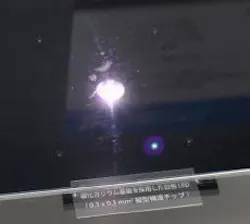
White LED has gallium oxide substrate, vertically placed electrodes
Tokyo, Japan--Tamura Corp. and Koha Co. Ltd.(which is owned by Tamura) have developed white LEDs that use gallium oxide (beta-type Ga2O3) as the substrate, and have exhibited them at Lighting Japan 2013 (Jan 16 to 18, 2013; Tokyo, Japan).
The main advantage of Ga2O3 over sapphire for substrates is that the semiconductor Ga2O3 is electrically conductive, allowing the use of a vertical electrode structure in which the anode and cathode are formed on the top and bottom sides of an LED chip. In contrast, sapphire substrates are insulating and require a horizontal structure in which the anode and cathodes are horizontally arranged.
Advantages of vertical structure
The vertical structure makes it easier to reduce element and heat resistances and to achieve an even current distribution. The lower the element and heat resistances, the less heat is generated by the LED chip. As a result, the new LED can be driven by a higher current.
The LED consists of a blue LED chip fabricated on a beta-type Ga2O3 substrate using a gallium nitride (GaN)-based semiconductor for the emitting portion, and a fluorescent material. The new LED has a higher optical output tan those based on sapphire substrates, the companies said.
At the show, Tamura and Koha exhibited two types of white LEDs that use 0.3 x 0.3 mm and 2 x 2 mm blue LED chips, respectively. Their driving currents are 400 mA and 6 A. The brightness of the LED using the 2 x 2 mm chip is about 500 lm; the companies aim to increase this to 2000 to 3000 lm—a level difficult to achieve using a sapphire substrate, they say.
Though GaN substrates are also suited for making high-output LEDs, beta-type Ga2O3 substrates result in lower costs, Tamura and Koha say. Currently, GaN substrates are manufactured by using hydride vapor-phase epitaxy (HVPE). But, beta-type Ga2O3 substrates are manufactured by the melt-growth method, which can potentially lead to larger, better-quality substrates.
Beta-type Ga2O3 substrates with a 2 in. diameter have already been commercialized; the two companies plan to create a 4 in. prototype in 2014 and commercialize it in 2015. They are also aiming to develop a 6 in. product.
Source: Tech-On!
About the Author
John Wallace
Senior Technical Editor (1998-2022)
John Wallace was with Laser Focus World for nearly 25 years, retiring in late June 2022. He obtained a bachelor's degree in mechanical engineering and physics at Rutgers University and a master's in optical engineering at the University of Rochester. Before becoming an editor, John worked as an engineer at RCA, Exxon, Eastman Kodak, and GCA Corporation.

