A year of the extraordinary
Single-atom lasers, tungsten photonic crystals, and other fundamental achievements vie for acclaim, along with commercial developments like visible fiber lasers, liquid lenses for cameras, and displays that capture images.
Most people understand that the well-worn Aesopian proverb, "Slow and steady wins the race," is flawed. Its laudable call to hard work ignores the fact that a flash of inspiration can move one scientist's research ahead of another's; a clever change in advertising tactics can mean millions to a commercial enterprise; and a risqué gesture in front of the right audience can help a pop singer climb the charts. The trick, of course, is to back the flashy move with the proper amount of preparatory and followup effort.
Along with much hard work, this year's advances in optoelectronics include some flashy moves—in the best sense. The resultant mix of invention and steady improvement is precisely what is needed to keep the field of optoelectronics moving along at its perennially brisk pace.
Pushing limits
Technological development deeply connected to basic science has made a strong appearance this year. The results may help to redefine technologies that are basic to the makeup of many optoelectronic systems.
Researchers at the California Institute of Technology (Caltech; Pasadena, CA) have created a single-atom laser that they call a "one-and-the-same-atom" laser, because the lone atom that serves as its optical gain medium does so for the entire period of lasing. This arrangement is in contrast to other single-atom lasers, which have to keep dropping atoms into the cavity as previous atoms escape. Because all photons emanate from the same atom, the photons in the Caltech laser have a quality called "antibunching," meaning they are spaced more evenly in time than random emission would dictate.1
In the laser, a cesium atom is held in place by a trapping light beam for a period on the order of 0.05 s. The resonant cavity is 42.2 µm long and has a finesse of 4.2 × 10⁵ at the laser's emission wavelength of 852 nm. The Caltech emitter—which, unlike normal lasers, has no threshold—has an output of somewhat under 100,000 photons per second and may one day be used in quantum systems for manipulating information. Although the term "antibunching" may not have much pizzazz, the Caltech device has redefined technological limits, having reached a level of optical noise lower than that for any laser yet built.
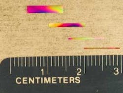
The emissive properties of surfaces are important to many optical systems, especially those that handle thermal loads. Researchers at Sandia National Laboratories (Albuquerque, NM) have created an emissive material unlike any other (see Fig. 1). Actually a photonic crystal, the material defies common views on what an emissive surface can do. While ordinary surfaces emit at a rate less than or equal to a perfect blackbody at all spectral points, the Sandia material can, for certain spectral ranges, exceed the performance of a blackbody.2
The photonic crystal is made of tungsten to allow heating to temperatures that cause it to emit in the near-IR and visible. It consists of square rods spaced 2.8 µm apart and stacked in alternately crossed rows, with offsets producing a stacking sequence that repeats every four layers. A complete metallic photonic band gap at wavelengths longer than 6 µm suppresses emission in that range. An enhanced photon-matter interaction at the band edge boosts emission within the 3- to 5-µm band; electrically heating the material to 1250∞C causes it to radiate in that range three times as efficiently as even a perfect blackbody. If the photonic crystal's band edge can be moved into the visible range, the result will be a greatly more-efficient incandescent light bulb; playing with its properties in other ways may allow thermal surfaces with tailored properties unlike any now available.
Tungsten has been used as a photon-counting detector by scientists at the National Institute of Standards and Technology (Boulder, CO) and Boston University (Boston, MA).3 The device, which has been shown to count photons at 670, 830, 1310, and 1550-nm wavelengths, is a superconducting transition-edge sensor that senses the heat produced by the absorption of single photons. It was used to verify the photon-number distribution (the rate of photon arrival versus time) of a weak pulsed laser-diode source at 1550 nm. The ability to tally up individual photons will aid in proving the security of quantum-cryptographic systems (see Laser FocusWorld, November 2003, p. 31).
A group led by Robert Boyd of the University of Rochester (Rochester, NY) has slowed light to a speed of 57.5 m/s at room temperature in a ruby crystal.4 A laser focused on the crystal burns a spectral hole and produces a refractive index that varies greatly as a function of wavelength for a narrow spectral band. The researchers have slowed both Gaussian-shaped pulses and amplitude-modulated optical beams. Although light has been slowed to similar degrees before, the techniques involved substances cooled to near absolute zero. The new result puts extreme slowing of light within reach of many optical laboratories.
Small visible lasers multiply
Lasers emitting visible light in the milliwatt range—ubiquitous in lab setups, life-sciences instrumentation, and consumer devices—are, in many ways, the consummate laser. Compact, easy to work with, and usually emitting in a single spatial mode, they produce small diffraction-limited spot sizes and have wavelengths valuable for spectroscopy, scanning, printing and imaging, and interferometry (to name just a few applications). The importance of this type of laser drives innovation; smaller size, higher efficiency, and more wavelengths are the result (see "Confocal microscopy relies on a variety of lasers," p. 67).
Ever since the gallium nitride (GaN)-based laser diode was introduced a few years ago, Nichia (Kaminaka, Japan), having invented the device and obtained many patents on it, has had a lock on the market. While Xerox (Stamford, CT) is pursuing blue semiconductor lasers, and Cree (Durham, NC) has a cross-licensing agreement with Nichia covering GaN-based optoelectronic technology, neither company has introduced a production commercial device. Now, Toshiba (Tokyo, Japan) has developed a GaN-based high-power laser that is intended for blue-violet-laser-based optical-disc systems. Its 200-mw output is, according to the company, optically quiet and stable enough for dual-layer-disc recording and high-speed recording, both of which require a more-powerful laser source than single-layer, standard-speed recording.
Barring GaN-based laser-diode development, which seems to be the province of large companies dedicated to semiconductor technology, small blue lasers can be created in other ways. The frequency-doubling of vertical-cavity surface-emitting lasers (VCSELs) or edge-emitting laser diodes—a trend that started a couple of years ago with the introduction by Coherent (Santa Clara, CA) of a doubled, optically pumped VCSEL—continues apace. Many of these lasers were developed specifically as a replacement for the 488-nm argon-ion laser, widely used in the biosciences for DNA sequencing and other applications.
Picarro (Sunnyvale, CA) has introduced its own version, a 20-mW, 488-nm device that contains a frequency-doubled external-cavity semiconductor laser. A single-spatial-mode laser diode in a thermoelectrically cooled external cavity emits 976-nm light; the frequency-doubling crystal is placed external to the cavity to simplify the control of the laser's stability. The company consulted closely with makers of bioscience instrumentation to ensure the laser will function well in DNA sequencers and flow cytometers. The company claims that the laser dissipates 30% to 50% less heat than most other solid-state-laser alternatives of that wavelength.
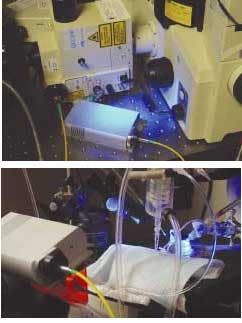
Blue Sky Research (Milpitas, CA) now has on the market a 488-nm-emitting frequency-doubled laser that is built around a telecommunications-grade 980-nm semiconductor pump laser (which meets Telcordia specs for reliability). The device has a 25-mW output and comes in both fiber-pigtailed and free-space-output versions. "The pump laser is fiber-pigtailed too, making for a rugged package," says Chris Gladding, the company's president and chief executive officer. The 145 × 82 × 33-mm laser operates on 5-V DC and requires only 12-W input power; an electrical connector allows users to remotely control the laser (see Fig. 2).
FIGURE 2. Researchers at the University of California San Francisco image live-cell fluorescence using 488-nm laser light. A fiber-coupled frequency-doubled laser from Blue Sky Research (top) was integrated by engineers at Solamere Technology Group (Salt Lake City, UT) into Solamere's spinning-disk live-cell imaging confocal microscope system. This application is a first attempt at measuring and capturing an image of the electric field as it transverses the heart during "normal" beating using a confocal microscope (bottom). The blue glow under the microscope is a mouse heart being exposed to 488-nm laser light to promote fluorescence. A CCD camera then captures the fluorescence image at 120 frames per second.
Visible low-power fiber lasers have made their commercial appearance, with German companies leading the way. Unique-m.o.d.e. (Jena, Germany) has developed an upconversion fiber laser in which an active fiber serves as the nonlinear medium; light from an IR laser diode pumps the fiber, which produces 10 mW of single-longitudinal-mode light at 491 nm. The device is aimed squarely at the life-sciences market and was developed by the company in cooperation with researchers at the University of Hamburg (Hamburg, Germany) and an unnamed German manufacturer of bioscience instrumentation.
Lumic (Berlin, Germany) has developed both blue- and green-emitting upconversion fiber lasers; their 470-nm blue laser, already a commercial product, emits up to 5 mW. It contains a gallium arsenide–based laser diode and an active fiber known as ZBLAN (containing zirconium, barium, lanthanum, aluminum, and sodium fluorides) doped with rare-earth ion mixtures; multiple rare-earth ions allow two separate stepwise absorptions of pump photons, producing a nonparametric frequency conversion. The resonator mirrors for the fiber laser are integrated into the fiber connectors. The company is producing its first samples of a 520-nm green upconversion fiber laser.
Spectra-Couleur (Berlin, Germany)—a year-old company spun off from the Technical University of Berlin—has introduced blue, green, and red fiber lasers with emission wavelengths of 491, 520, and 635 nm, respectively. While rated for a 10-mW output, the devices are capable of emitting several hundred milliwatts, according to Volker Gäbler, one of the company's founders.
One visible fiber laser that most certainly does not qualify as low power was introduced by IPG Photonics (Oxford, MA) earlier this year; the frequency-doubled erbium laser is tunable between 770 and 780 nm and produces 5 to 30 W of light in 3-nm pulse at up to a 20-MHz repetition rate. It should be noted, though, that the laser's output is at the extreme long-wavelength edge of the human eye's ability to perceive light, so its uses will not include those having to do with vision, such as image projection. It will find use instead in drilling, micromachining, science, and medicine.
All-seeing electronic eyes
This year has seen engineering improvements to many types of imaging devices. For instance, the standard indium gallium arsenide (InGaAs) IR camera is sensitive over a 900- to 1700-nm spectral range—adequate for many applications, but not for those that mix visible with IR. While some detector materials (notably mercury cadmium telluride and indium antimonide) cover an IR-visible region, they are expensive. Indigo Systems (Goleta, CA) has introduced a method of processing standard InGaAs detector material that pushes its short-wavelength response across the visible to 400 nm (see Fig. 3). Dubbed VisGaAs by the company, the new detector type is the basis for thermoelectrically cooled 320 × 256- and 640 × 512-pixel cameras that can be used in spectroscopy, daytime/nighttime covert surveillance, and laser-based applications using, for example, the 850-nm wavelength.
A high-speed CMOS motion camera developed by Redlake (San Diego, CA) achieves frame rates of 1000 frames/s at its maximum 1504 × 1128-pixel resolution, and rates of up to 100,000 frames/s at a reduced resolution—speeds traditionally seen only in CCDs. The camera has a 5-µs shutter to freeze motion of extremely high-speed events and, in keeping with its intended use in harsh environments, is designed to withstand forces of 100 G in any axis. A Gigabit Ethernet hub allows remote control of the camera as well as downloading of images to servers and handheld devices. Applications so far have included the measurement of insect locomotion, which may lead one day to the creation of adept many-legged robots.
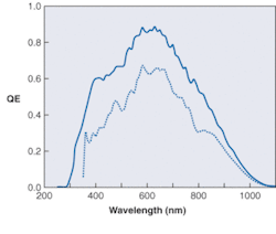
In a blue-enhanced line of CCDs introduced a few years ago by Eastman Kodak (Rochester, NY), one of the polysilicon electrodes used in full-frame sensors was replaced with a much more transparent indium tin oxide (ITO) material, raising blue-light transmission. The other electrode had to remain polysilicon, however. Now, Kodak has further boosted efficiency by placing a microlens array—one lens per pixel—over the CCD sensor. The array focuses light mostly onto the more-transparent ITO electrode, boosting quantum efficiency from 30% to 60% at 400 nm and substantially as well across the visible spectrum (see Fig. 4). This improves on earlier techniques, in which high levels of quantum efficiency were reached only through an expensive process of thinning the wafer and illuminating the image sensor from the backside. The 2184 × 1472-pixel monochrome camera is sensitive to the 300- to 1000-nm spectral band and has a room-temperature dynamic range of 75 dB.
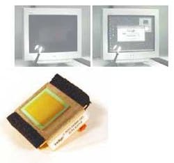
Toshiba America Electronic Components (Irvine, CA) has demonstrated what it calls an "input display," which captures images directly with sensors built into its thin-film-transistor liquid-crystal display (LCD). A 3.5-in.-diagonal low-temperature-polysilicon full-color LCD with a 320 × 240 resolution contains three light detectors per display pixel, enabling a 960 × 240-resolution image capture either of objects placed directly against it, or of projected images. If built into a PDA, the input display could capture data from a catalog, read barcodes, or recognize and authenticate fingerprints.
Varioptic (Lyon, France) has introduced a fast-focusing liquid lens for CCD cameras that contains two immiscible liquids in a windowed cell (see Laser FocusWorld, November 2003, p. 17). Varying a voltage changes the "electrowetting" properties of the liquid/liquid interface where it contacts the cell, making the interface more or less wettable against the cell and changing the interface's radius of curvature. The lens can focus through a focal range of -200 mm to infinity to +50 mm within 0.03 s and is lightweight, small, and rugged enough to serve as an autofocus device for consumer digital cameras.
EUV lithography
In the optics-heavy area of integrated-circuit manufacture, Intel (Austin, TX) dropped 157-nm lithography from its roadmap, aiming instead to extend 193-nm lithography down to 45-nm feature sizes, beyond which extreme-ultraviolet (EUV) lithography would take over. The move, which included Intel's pushing its use of EUV back from 2007 to 2009, sent shock waves throughout the industry, causing a general reevaluation of and backing away from 157-nm lithography. As a result, EUV lithography, with its 13.4-nm wavelength, is now a greater focus of interest than it was.
A few years ago, a consortium of U.S. semiconductor manufacturers called EUV LLC kick-started the development of EUV technology in the United States; more recently, Japan has gotten into the game, with excimer-laser maker Komatsu, light-source specialist Ushio, and their joint effort Gigaphoton (all of Tokyo, Japan) forming a cooperative EUV-source program. Japan's two largest makers of lithographic steppers and scanners are Nikon (Kanagawa) and Canon (Utsunomiya); these two companies, which together dominate the world stepper market, are intensely pursuing EUV technology.
In just one example of this pursuit, a group of Nikon engineers is developing beam-homogenizing optics to meet the exacting specifications of EUV systems.5 A "fly-eye" beam homogenizer receives a nonuniform beam, breaks it up into small portions, and then overlaps the portions to achieve the beam uniformity needed to create features of consistent size across a chip. Because the beam passing through the off-axis reflective EUV optics is arc-shaped, the beam homogenizer contains about 500 arc-shaped concave elements side-by-side. The engineers looked at various ways of fabricating this complex optical element, selecting an element-by-element fabrication process (see Fig. 5). They fabricated elements from Invar with nickel-plated surfaces and investigated their surface quality (accurate to 0.31-µm peak to valley), profile accuracy, and slope accuracy. The next step for the group will be to assemble the elements into a complete array.
And much more
The first commercial terahertz spectrometer was launched this year by Bruker Optics (Coventry, England) and TeraView (Cambridge, England). Terahertz spectra can reveal the makeup and characteristics of human tissue, plastics, and semiconductors; the radiation can penetrate clothing, paper, and cardboard and reveal the presence and type of substances beneath, such as explosives (see Laser FocusWorld, July 2002, p. 23). Applications include medical imaging and diagnosis, life-sciences applications such as drug discovery and proteomics, food and beverage analysis, nondestructive testing, and security (see Laser FocusWorld, April 2003, p. S12).
In the instrument, an ultrafast laser produces pulses that generate broadband terahertz radiation when they strike a semiconductor crystal. The terahertz radiation is directed to the specimen, which reflects the radiation from its internal structure. From coherent detection of the time-delayed reflections, a three-dimensional image is constructed; mathematical operations produce the specimen's absorption spectrum for each point within it, helping to determine the chemical composition.
Researchers at OmniGuide Communications and the Massachusetts Institute of Technology (MIT; both of Cambridge, MA) continue to refine and find new uses for the hollow light-guiding fiber produced by OmniGuide. The fibers are lined on their inner surface with a multilayer high-reflection coating consisting of alternating layers of chalcogenide glass and polyethersulfone (a polymer); the large difference in the two materials' refractive indices produces a reflection close to unity across a wide band of wavelengths and for all incidence angles.
One use the researchers are pursuing is dispersion tailoring and compensation.6 This effect of the fiber relies on weak interactions between its core-guided mode and a mode localized in an intentionally fabricated crystal defect (multilayer thin-film coatings are one-dimensional photonic crystals). The high index difference between the air core and the multilayer cladding results in dispersion parameters in excess of 500,000 ps/nm-km. The phenomenon is tunable by altering the fiber's drawing speed and structure; the dispersion slope can be matched to that of commercial silica fibers to better than 1%, or can be made zero. In addition, the nondegenerate TE01 mode—which is the lowest-loss mode for the fiber—is immune to polarization-mode dispersion.
In the field of dense wavelength-division multiplexing, the reconfigurable optical add/drop module (ROADM) appears to be headed for wider use (see Laser FocusWorld, November 2003, p. 54). Clarendon Photonics (Newton, MA) has developed monolithic single-chip ROADMs—one four-wavelength version that includes a variable optical attenuator (VOA) and one eight-wavelength version with no VOA (see Fig. 6). The chip of the eight-channel version is one-quarter the size of a Pentium 4 microprocessor and can be configured for add/drop filtering and dynamic switching; by integrating additional components onto the chip, VOA functionality and a monitor tap could be added to the basic eight-channel unit. Because the devices are monolithic, the company can develop increasingly complex devices simply by changing the layout of the lithographic photomask.
REFERENCES
- J. McKeever et al., Nature 425 (September 18, 2003).
- Shawn-Yu Lin et al., Appl. Phys. Lett. (July 28, 2003).
- A. J. Miller et al., Appl. Phys. Lett. (July 28, 2003).
- M. S. Bigelow et al., Phys. Rev. Lett. 90, 113903 (2003).
- H. Takino et al., Opt. Engineering, 9 (September 2003).
- T. D. Engeness et al., Optics Express 11(10) (May 19, 2003).


