Diamond-based LED emits ultraviolet light
Researchers at the National Institute for Materials Science (Tsukuba, Japan) have reported the realization of an ultraviolet (UV) light-emitting diode with the use of a diamond p-n junction.1 The wide energy bandgap of diamond (5.47 eV) is promising for optoelectronic applications because it allows the possibility of UV LEDs, an important step toward diamond lasers, UV fluorescence lighting, and high-density data storage. In addition, diamond-based LEDs have the advantage of extreme durability compared to other semiconductor materials.
Satoshi Koizumi and colleagues formed the p-n junction from a boron-doped (b-doped) p-type diamond layer and another phosphorus-doped (p-doped) n-type diamond layer. The b-doped and p-doped diamond thin-films were independently grown via microwave plasma-enhanced chemical-vapor deposition on the mechanically polished <111> surface of a b-doped single crystalline diamond. The films were grown using trimethylboron and phosphine as impurity source gases.
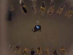
Ohmic electrodes were formed for both the p-type and n-type layers. On the p-type layer, the scientists deposited a 100-nm thick film of titanium protected with a gold evaporated film. On the n-type layer, argon ion implantation through a mask formed about two dozen graphitic dots 30 nm deep and 150 µm in diameter (see Fig. 1). The implanted dots also were covered by titanium and capped with gold film for protection.
The diode's light-emitting properties were tested by applying increasing voltages to it. At voltages exceeding 0.1 mA, the team noticed light emissions around the electrodes over a range of UV and visible wavelengths. As the forward current was increased, they observed a peak in UV light emission located at 235 nm (see Fig. 2).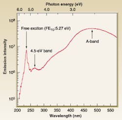
The UV luminescence at 235 nm (5.27 eV) is attributed to free exciton recombination, assisted by the transverse-optical phonon transition of non-doped high-quality diamond. The peak energy of the luminescence is considerably higher than that observed from gallium nitride at 357 nm (3.47 eV). Broadband emission in the visible region is attributed to A-band emission often observed in analysis of chemical-vapor-deposition diamond thin-films. The researchers predict that improving the crystalline quality of the b-doped layer will suppress the A-band emission to create monochromatic UV light from a diamond LED.
REFERENCE
- S. Koizumi, K. Watanabe, M. Hasegawa, and H. Kanda, Science 292, 1899 (2001).
About the Author

Valerie Coffey-Rosich
Contributing Editor
Valerie Coffey-Rosich is a freelance science and technology writer and editor and a contributing editor for Laser Focus World; she previously served as an Associate Technical Editor (2000-2003) and a Senior Technical Editor (2007-2008) for Laser Focus World.
Valerie holds a BS in physics from the University of Nevada, Reno, and an MA in astronomy from Boston University. She specializes in editing and writing about optics, photonics, astronomy, and physics in academic, reference, and business-to-business publications. In addition to Laser Focus World, her work has appeared online and in print for clients such as the American Institute of Physics, American Heritage Dictionary, BioPhotonics, Encyclopedia Britannica, EuroPhotonics, the Optical Society of America, Photonics Focus, Photonics Spectra, Sky & Telescope, and many others. She is based in Palm Springs, California.