Resist outgassing challenges loom at 157 nm
As photolithography tool manufacturers hone in on 157-nm wavelengths, they will also need to optimize purge-flow systems and material chemistry to prevent lens contamination caused by condensation of gasses that form as a result of photoresist exposure to laser light, according to International Sematech research presented in March by Stefan Hien at the annual SPIE Microlithography symposium in in San Jose, CA. The multimillion dollar investment that goes into photolithography tools comes with the expectation of five- to ten-year lifetimes that could be shortened to several months, he said, if the more stringent demands of 157-nm operation are not taken into consideration.
Deposition from photoresist outgassing can change the optical behavior of the lens in the photolithography tool, Hien said. "If you have an additional layer that is not homogeneous over the lens surface you don't have the focus anymore," he said. "It detunes the lens. So the quality of your image can get very bad."
Managing outgas deposition is expected to be more challenging at 157 nm than in previous generation tools at 248 and 193 nm for a couple of reasons. At the higher energy (7.9 eV) for 157 nm, direct laser cleavage of organic particles generates volatile deposition precursors. Also the atmospheric purification provided at 248 and 193 nm by ozone generated from ambient oxygen is expected to lessen significantly at 157 nm because air is not transparent to the vacuum ultraviolet (VUV) light at 157 nm and the chamber must be nitrogen purged, pushing oxygen concentrations down to the part-per-million range. One factor that must be evaluated is the deposition rate of laser generated outgassing species from the gas phase. "We have to understand what's going on at a new wavelength," Hien said.
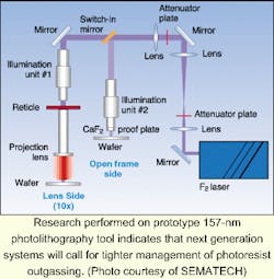
To evaluate potential problems and investigate management strategies, researchers from International Sematech (Austin, TX), MIT Lincoln Laboratory (Cambridge, MA) and Exitech Limited (Oxford, England) collaborated to perform a risk assessment experiment using a prototype 157-nm tool (see figure).
First, outgassing was measured as a function of film thickness loss. Thickness loss from a 200-nm thick polymer film ranged from 5 to 30 nm depending on the polymer material under 100 mJ/cm2 of 157-nm radiation.
Second, the molecular fragmentation between the lens and the wafer was measured using a complex device built at MIT Lincoln Lab that combined both the nitrogen purging exposure chamber for 157-nm with a mass spectroscopy system for measuring the atomic distribution. While they did not find outgassing rates at 157-nm to be significantly different from that at 248-nm and at 193-nm, the researchers did find a broader variety of compounds generated, with benzene being the predominant compound, as at the other two wavelengths. In the third step outgas deposits on a dummy lens were collected by a couple of methods, of which, x-ray photoelectron spectroscopy (XPS) proved the most sensitive. The XPS measurements were taken before and after the etching process.
"You may find silicon or you may find sulfur or you may find organic fluorine there," Hien said. "And this is a clear indication that the deposit is coming from the resist that has been used on the wafer at a certain distance from the plate, which is a clear proof of the transport to the surface."
The researchers found that outgassing could be minimized by judicious choice of film material and that ozone purging of fluorine contaminants could still take place at the relatively low oxygen concentrations required for 157-nm operation. Silicon contaminants could not be cleaned in this manner, however, and Hien emphasized that in addition to chemical steps to minimize outgas deposition, optimization of the proprietary purging systems within the photolithography tools, such as the radial symmetric purge and the cross-field purge, will still play a major role.
"This is the challenge of the future," he said.
About the Author
Hassaun A. Jones-Bey
Senior Editor and Freelance Writer
Hassaun A. Jones-Bey was a senior editor and then freelance writer for Laser Focus World.