The Massachusetts Institute of Technology (MIT; Cambridge, MA) has committed to build a new fabrication facility for MIT Microphotonics Center researchers. The new facility will add the capability of fabricating dielectric and compound semiconductor materials for optical components. This will be the first dedicated physical area belonging to the relatively new center.
The goal of the center is to develop integrated optical devices to replace discrete components, with researchers now focusing on areas of research that include photonic bandgap crystals, developing integrated optics on silicon, using light on the chip level to relieve data I/O bottlenecks, development of organic materials for photonics, and developing devices such as ring resonators.
Center director Lionel Kimerling explains that the 20-member core faculty hails from a broad range of departments, from aeronautics to business management, as well as chemistry, physics, and chemical, materials, and electrical engineering. The center receives funding both for precompetitive research through the Industry Consortium and for specific R&D projects through alliances with industrial sponsors.
A Consortium-level project currently under way is the center-wide Microphotonics Technology Roadmap that will be available to all center sponsors. The Roadmap is looking at applications of light (including optical computing and networking), at drivers for the technology, and at how fast the area is developing. Charles Fine from the Sloan School of Management and Rajeev Ram from Electrical Engineering and Computer Science are leading the effort.
Materials science issues, including the development of new materials and processes, resonant structures and devices, and integrated functionality are key areas of research. Many of the materials-science-related aspects of the center's work were reported recently at last fall's meeting of the Materials Research Society (MRS; Boston, MA).
Photonic crystals
Photonic crystals are artificial periodic structures that provide bandgaps within which light of a certain frequency range cannot propagate (see Laser Focus World, September 2000, p. 133). Just as semiconductor bandgaps have been used for years to manipulate and control electrons, photonic crystals can be used to confine and control photons. Such devices could be used to extract light efficiently from diodes, as wavelength-selective add/drop filters, lossless waveguides, or very-high-efficiency cavities that could form the basis of nano-sized lasers.1 The researchers are working in silicon and other compound semiconductor systems to develop these systems. An omnidirectional reflector (based on a dielectric stack mirror) developed by a group of researchers, which includes John Joannopolous, Edwin Thomas, and Yoel Fink, is being commercialized by a company called OmniGuide Communications Inc. (Cambridge, MA). The reflector can be formed into a hollow cylinder to provide a highly efficient air-core lightguide. The company is working on further development, optimization, and fabrication of the guide.
Silicon microphotonics
Another group at the Microphotonics Center is working on incorporating light with electronics at the chip level. Kimerling explains, "As transistors get smaller, the propagation delay increases" due to capacitance and other effects. In one project, researchers are investigating the use of light to transmit the clock signal in a computer. By coupling 1.5-µm light from an external source into low-loss high-confinement submicron waveguides to monolithically integrated germanium detectors, the researchers are developing an optical bus that can be used to overcome the data I/O bottlenecks that currently exist in microelectronics. Jessica Sandland and others describe work on optimizing silica-on-silicon optics at MRS, and Hsin-Chiao Luan and others authored an MRS paper on germanium photodetectors for integration with silicon.2, 3
Also at the MRS meeting Michal Lipson reported on her work developing CMOS-compatible microemitters for silicon.4 Thus far, optics on silicon has mostly been confined to passive devices. If active optical devices—including lasers or at least efficient light emitters—could be made on silicon, "it could change the whole face of electronic chips today," says Lipson. She is using microcavities in silicon to boost the efficiency of an erbium-doped gain material, in an attempt to create lasers that can be fabricated as part of a silicon chip.
Organic materials
Other researchers at the center are developing organic materials for optical purposes. Kimerling mentions work on self-assembly for photonic crystals, LEDs, and large-area displays.5 One example involves the use of quantum dots to manipulate the refractive index of a material in order to create an organic photonic crystal. For example, if two different polymers (or a block copolymer with suitably different regions) are mixed, at equilibrium they may phase-segregate and form useful structures. Once the structures exist, the index of one phase can be increased by infiltrating the material with quantum dots that have been modified to bind specifically to that phase.
Coupling
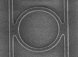
Other work involves investigating connections and coupling with the aim of reducing or eliminating insertion loss. Ring resonators, borrowed from microwave technology, are promising devices with fairly straightforward telecom and WDM applications (see figure). Assuming that the rings are fabricated well enough, they can provide waveguide coupling at the resonant frequency, "with essentially no loss," says Kimerling. Therefore, these structures could be used as wavelength-selective filters.
In addition to materials science, the faculty thus far brings to the group expertise in fabrication, design, and optical network architecture, as well as a commitment to interdisciplinary collaboration. "As director," says Kimerling, "I want to bring in as many faculty as possible" to the center.
REFERENCES
- Alexei A. Erchak et al., Proc. Mat. Res. Soc. Fall Meeting 2000, paper E2.8.
- Jessica Sandland et al., Proc. Mat. Res. Soc. Fall Meeting 2000, paper E5.23.
- Hsin-Chiao Luan, Douglas D. Cannon, Kazumi Wada, and Lionel Kimerling, Proc. Mat. Res. Soc. Fall Meeting 2000, paper E5.6.
- Michal Lipson, Kevin Chen, Sajan Saini, and Lionel Kimerling, Proc. Mat. Res. Soc. Fall Meeting 2000, paper E2.5.
- Yoel Fink et al., Proc. Mat. Res. Soc. Fall Meeting 2000, paper E4.3.
