Not only are charge-coupled-device (CCD) production levels currently in the hundreds of millions units, but their performance levels are already close to the limits dictated by physics. For these reasons alone, it may be difficult to see how these imaging devices could be improved further. Still, manufacturers have a clear incentive to do so—competition from complementary-metal-oxide-silicon (CMOS) imagers that are intrinsically simpler and cheaper to build.
Quieting the noise
The key to high performance in CCDs is noise reduction. A lower noise level translates to a more-sensitive detector with more-reliable readout. The problem is that there are a number of distinct types of noise, each with its own causes and cures.
Dark current noise, for instance, occurs when there is no light present. The main sources of such noise are from thermal generation in the potential well, the bulk material, or at the silicon/silicon-dioxide surface. In all three cases, the thermal motion of the atoms can release excess charges that have been generated or trapped by defects and impurities.
Also in this category is fixed pattern noise, often termed dark-signal nonuniformity. Fixed pattern noise occurs when the amount of dark current noise differs from one pixel to another, depending on nonuniformities in doping level, oxide layer thickness, or other parameters. This can create spurious local signals, instead of just a constant fog across the whole image.
In addition to dark current noise, device users must deal with pixel nonuniform response. Here, the amount of charge produced by a given quantity of photons varies from pixel to pixel, producing noise only when there is illumination. Another problem is amplifier noise generated by the analog circuitry that converts the electrons output from the CCD into a voltage signal.
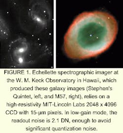
The most straightforward approach to combating noise is to cool the CCDs to reduce the thermal agitation. Dark current decreases by about a factor of two for each 8°C to 9°C drop in temperature. At liquid-nitrogen temperatures used in some applications, such as astronomy, dark currents can drop as low as one electron per pixel per hour. Even at -45°C, dark currents are only around 10 times this level (see Fig. 1). In addition, manufacturers are continuously reducing the number of defects, thus cutting noise. Currently, dark current density at room temperature ranges from 0.1 to 10 nA/cm2 depending on the manufacturer.
Amplifier noise, which is generated by the transistors that reset the output voltage after each charge measurement, can be counteracted by correlated double sampling, which measures and subtracts the reset noise from the total signal to yield the true video signal. Remarkable progress has been made in reducing amplifier noise until errors now run as low as a few electrons per measurement. (A full CCD well in a given pixel can have as many as 100,000 electrons.)
Extending CCD range
Although CCDs can view near-infrared (NIR) radiation to about 1.1 µm, scientists are also working to extend their range by combining the devices with other technologies. One example involves the use of night-vision cameras at room temperature, which can link CCDs with gallium-arsenide (GaAs) image intensifier tubes.
In this technique, a GaAs photocathode generates photoelectrons from short-wave infrared (IR) radiation. A multichannel plate helps multiply the number of electrons in a process that causes the electrons to produce secondary showers from the walls of each channel. The electrons then convert to visible light as they strike a phosphor. A CCD mounted behind the phosphor records the resulting visible light image. Such combinations of different technologies, however, are limited in resolution since spot size tends to be at least 100 µm and efficiency is relatively low.
There are also several techniques for improving CCD performance at short wavelengths. One involves flooding the device with intense ultraviolet (UV) light before exposure. The UV photons stimulate the emission of electrons in the bulk silicon, and some of these electrons migrate to the backside surface and are trapped in its oxide layer. This condition creates a negative potential that pushes photoelectrons emitted during exposure toward the storage wells. Gases such as chlorine or nitric oxide produce similar results.
The advent of the super CCD
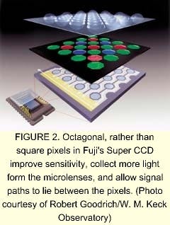
The continuous efforts to bolster CCD performance are already bearing fruit. Perhaps one of the most significant recent improvements involves Fuji Photofilm's Super CCD image sensor, a device introduced early last year for the digital photography mass market.1 While conventional CCDs use vertical square arrays of pixels, the Super CCD has octagonal-shaped pixels with output lines tilted at 45° to the vertical (see Fig. 2). Both resolution and effective speed, or exposure index, are double that of older CCDs.This new pixel arrangement has several advantages. For one thing, the octagonal shape is closer to the circular patch of light created by the microlenses that focus light on each pixel, so less light is wasted. In addition, the control signal path cuts diagonally from pixel to pixel, instead of running along the top of the line of pixels. This allows a larger area per pixel, which naturally leads to greater sensitivity to light.
Fuji engineers tilted the whole array at 45° to the vertical to reduce the spacing between pixels in both the vertical and horizontal directions. Studies of human vision have shown that maximizing pixel resolution, even at the expense of resolution in the diagonal directions, improved image quality.
CCDs vs CMOS
While CCDs still dominate the imager market, they face serious competition from CMOS imagers. Because they benefit from the enormous previous investment in DRAM memory chip manufacturing capacity, CMOS devices are extremely cheap to produce. This fact has led to an explosion in new designs of products with CMOS, rather than CCD imagers.
In contrast, CMOS imagers expose a line at a time and then transfer that line into an output register. This can be a disadvantage with rapidly changing scenes since objects in rapid motion appear tilted and distorted.
Charge-coupled devices still have significant advantages in a number of areas.2 For one thing, in frame-transfer CCDs, all the pixels are exposed at one time, and their electron contents are then transferred in one operation into a frame memory, which is not exposed to light. The standard, bucket-brigade transfer of electrons from pixel to pixel then empties the frame memory sequentially. This means that the resulting image is a snapshot of the scene, just as it is with film.
The higher production costs and complexity of CCDs (the elements are duplicated in the frame memory) translate into greater fidelity for rapid motion. These devices also have lower dark noise levels than CMOS imagers, and so have greater sensitivity and greater dynamic range—the ratio between the darkest and brightest lights that can be recorded. Dynamic range is important in most scientific applications and in general photography to give any photo a relatively life-like appearance. The reason is that the eye's dynamic range is far beyond that of any imager. The larger the dynamic range, the more the scene resembles what we see.
Also, CCDs can be built into mosaic arrays, which allow the production of very large imagers. The devices thus work well in higher-resolution applications where the image is spread out over many millions of pixels.
Advantages such as these will almost certainly ensure that CCDs maintain a large, perhaps dominant position in the image sensor market for a long time to come.
References
- J. Larish, Adv. Imaging 15, 18 (January 2000).
- D. Lake, Adv. Imaging 15, 12 (January 2000).
Decomposing CCD structure
CCD arrays are built up out of pixels consisting of metal oxide-silicon (MOS) capacitors. Each of these is an insulating silicon-dioxide layer over a p-type silicon substrate that is capped by a thin metal electrode. With an applied bias, holes move away from a depletion layer in the silicon beneath the gate, creating a potential energy well. Electron-hole pairs are generated when the device is illuminated and the electrons accumulate in this well, with the accumulated charge proportional to the irradiation. Charge readout involves sequential transfer of the charge from pixel to pixel until it is detected at the edge of the CCD chip.
About the Author
Eric J. Lerner
Contributing Editor, Laser Focus World
Eric J. Lerner is a contributing editor for Laser Focus World.
