Communication port density hinges on efficient EMI design
In an era when optical communications system designers are being pressured to move toward lower cost, higher capacity, and scalability, increasing the number of signals that can be transmitted or received through the same physical space is generally considered a good thing. So manufacturers of small form-factor pluggable (SFP) optical transceivers are expecting a strong market demand because SFPs allow manufacturers of network equipment to increase port density by placing the devices closer together than would have been possible with larger transceivers, such as pluggable gigabit interface converters.
In addition to the physical footprints of SFP devices, however, design considerations for operating transceivers at higher port densities must also take into account factors such as electromagnetic interference (EMI), which might be thought of as one dimension of the energy footprint. Thermal dissipation might be thought of as a second dimension. Of the two, EMI presents specific design limits regulated by the Federal Communications Commission (FCC) in the United States and by corresponding agencies in other parts of the world.
The FCC limits on EMI emissions from digital electronic devices connected to fiberoptics (classified as "unintentional radiators") are 49.5 dB µV/m measured at 10 m in industrial environments and 54 dB µV/m measured at 3 m in residential environments (6 dB lower than industrial). The limits apply to individual transceivers and to the network equipment boxes in which they are placed. The design criteria for minimizing EMI emissions in individual transceivers and in network equipment boxes are the same but the measurement systems differ.
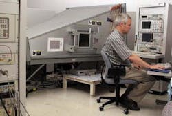
Emissions from network equipment boxes are evaluated for FCC compliance in an open-air test site, while individual SFP transceivers are tested in a gigahertz transverse electromagnetic (GTEM) cell, which Steve Hart from the semiconductor products group at Agilent Technologies (Santa Clara, CA) describes as an anechoic chamber (see figure). Limitations such as background noise in the open-air test can produce a standard error on the order of 3 dB, while the controlled GTEM environment facilitates precise measurements in a simulated network box, which isolate the radiation from the SFP vs. background emissions, according to Hart.
"We create the ideal customer box," he said. "It's essentially a noiseless, 0-dB box. And we're left with maybe a 1-dB measurement error. Then we can calculate how many SFPs we would be able to put into a perfect customer box." The measurement is typically performed in two ways—closed and open box. The closed box measurement simulates a noiseless box with one transceiver in it. The open box measurement introduces background noise that would be encountered in a real-world network equipment box.
Hart lists several EMI design considerations that apply to both transceivers and system boxes. The first level involves minimizing current flow to radiative sources. For example, since they generally have lower drive currents, "VCSEL-based sources are lower radiators than edge-emitting or Fabry-Perot laser-based sources, and thus multimode transceivers will tend to have lower EMI potential in general than single-mode sources," he said.
The next design consideration is shielding, which relies in no small part on the art of making metal-to-metal contact between the transceiver and the network box. "If you don't actually make contact with the box, you don't shield radiation that's inside the box from getting outside the box and it becomes a weak point or a potential radiator," Hart said.
Further along the design hierarchy one encounters good printed circuit-board (PCB) design and impedance matching. "Long signal traces are good sources of radiation, particularly if they are carrying common-mode current instead of differential current," he said. "What you really want are short traces that are well impedance-matched and balanced. We tend to bury, and suggest to customers that they bury differential lines between power and ground planes or between ground planes in the PCB, instead of having them run along the top layer of the PCB."
Beyond equipment design considerations, one also encounters the radiative potential of the signals themselves. For instance, EMI emissions can be lessened by choosing idle patterns with lower spectral content from among the available idle patterns for various applications.
The ultimate goal is to design components to provide substantial system- design margins beneath the FCC limits. "EMI is something that we design in," Hart said. "We don't expect customers to spend a lot of time trying to justify or qualify the box."
About the Author
Hassaun A. Jones-Bey
Senior Editor and Freelance Writer
Hassaun A. Jones-Bey was a senior editor and then freelance writer for Laser Focus World.
