Photonic bandgap channels waves propagating at metal surfaces
Researchers at Aalborg University (Aalborg, Denmark) and the Technical University of Denmark (Kongens Lyngby, Denmark) have directly observed a bandgap effect in surface plasmon polaritons (SPPs) that may eventually play an important role in optical integrated circuits. Photonic bandgaps (PBG), the optical analogy of electronic bandgaps in semiconductor materials, have been previously observed in photonic crystals and holey fibers, where a periodic modulation of the dielectric constant resulted in the forbidden gap in the radiation spectrum. Consequently, structural irregularities, such as line defects, in such a dielectric lattice have acted as waveguides for specific wavelengths of light.
"Using the language of physical optics, the PBG effect can be viewed as an extension of Bragg reflection in one direction to Bragg reflection of waves propagating in any direction," according to Sergey Bozhevolnyi of the Institute of Physics at Aalborg University. "The PBG effect in periodic media can also be regarded as a counterpart of strong (Anderson) localization of light in random media, both being interference phenomena related to strong multiple scattering of light."
Bozhevolnyi was lead author of a recently published article describing the successful extension and direct observation of the bandgap effect in surface plasmon polaritons: the surface propagation of electromagnetic waves along the interface between a metal surface and a dielectric material.1 Bozhevolnyi and his team used scanning near-field optical microscopy (SNOM) to observe the waveguide effect of their SPP band-gap structure.
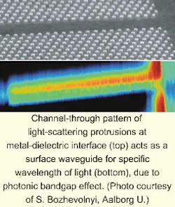
The rest of the experimental apparatus consisted of a 45-nm-thick gold film thermally evaporated on a glass substrate and covered with a triangular pattern, deposited using electron-beam lithography, of 200-nm-wide and 45-nm-high gold bumps with a 400-nm period. Bandgap waveguides were introduced into the light-scattering lattice in the form of line defects of various orientations and widths (see figure). Orientations of line defects were either parallel to the orientation of the lattice lines or parallel to the chains of hexagonal clusters, producing either smooth or corrugated waveguide walls, respectively. Three defect widths were used: two rows of bumps (800 nm), three rows of bumps, and 3.2 µm. The light source consisted of p-polarized light from a Ti:sapphire laser providing 50 mW of output in a 300-µm spot at wavelengths from 780 to 820 nm. The light was coupled to the gold surface through a glass prism.
The researchers observed that SPPs produced by 782-nm light were blocked by the lattice structure, whereas SPP intensity inside the lattice increased rapidly with increases in wavelength to 792 and 815 nm, which the researchers interpreted as a strong evidence of the photonic bandgap effect. The SPP propagation within line defects did not occur in the two-row-width smooth waveguide or in the three-row-width corrugated waveguide. But it was observed in the three-row-width smooth waveguides and the 3.2-µm corrugated waveguides, indicating that the smaller waveguide channels may have been just below the width threshold for propagation of the fundamental mode, according to the researchers.
Single-mode propagation was observed in the three-row-width channel over a distance of only about 5 µm due to strong attenuation, while a multimode signal in the wider channel propagated over the full 18-µm length without noticeable attenuation. Next steps for the research include investigation of other photon bandgap phenomena such as propagating light around corners, and ultimately the researchers hope that the SPP surfaces might be coupled to diffraction gratings and optical fibers for use as optical integrated circuits.
REFERENCE
- S. I. Bozhevolnyi, J. Erland, and K. Leosson et al., Phys. Rev. Lett. 86(14) 3008 (April 2, 2001).
About the Author
Hassaun A. Jones-Bey
Senior Editor and Freelance Writer
Hassaun A. Jones-Bey was a senior editor and then freelance writer for Laser Focus World.
