The first high-volume maker of a reliable low-cost, blue-emitting laser diode will reap vast rewards. Such a device would inevitably become the standard laser in next-generation digital versatile disc (DVD) data-storage devices, increasing DVD storage density by more than a factor of two. The only existing producer of blue-emitting gallium nitride (GaN)-based diodes, Nichia Corp. (Tokushima, Japan), can make long-lived (10,000-hr specified lifetime) GaN lasers, but can't make them inexpensively. The Nichia laser has thus found application mainly in spectroscopy, computer-to-plate setters, and other niche uses.
The Nichia devices are fabricated by growing GaN-based layers on a sapphire substrate; the company has developed processes, portions of which remain undisclosed, for making long-lasting lasers. A second approach pioneered by Cree (Durham, NC) entails growing the same sorts of layers, but on a silicon carbide (SiC) substrate; Cree is in the process of developing its own bag of tricks to lengthen device lifetime and raise output power. The use of SiC as a substrate results in an intrinsic increase in power handling and reliability as a result of the material's high thermal conductivity, according to Cree.
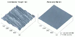
Gallium nitride-based laser diodes are expensive in part because tiny defects in the GaN material, which hinder the lasers' operation, are hard to eliminate in manufacture. With all its qualities as a good substrate, SiC itself can, however, induce defects in GaN.1 This occurs because commercial SiC wafers are covered with steps, typically one to eight atoms high, despite careful polishing by their manufacturers. The steps, which are simply the result of a slight but unavoidable tilt of the polished wafer surface with respect to the crystal's basal plane, act as nucleation sites for defects in GaN layers subsequently grown on the surface.
Researchers at the NASA Glenn Research Center (Cleveland, OH) have solved the step problem by developing a method of growing atomically flat surfaces on device-sized SiC mesas on wafers (see figure).2 They flatten ordinary stepped SiC surfaces by epitaxially growing more of the material, but under controlled conditions that limit crystal growth to the sides, or "risers," of the steps. The steps grow sideways until they reach the edge of the mesa, leaving a surface without a single step even one atom high.
Screw dislocations
The wafers themselves do not have perfect crystalline qualities. In particular, screw dislocations—or areas of helical atomic layering—are scattered throughout the wafer, according to Tony Powell, a senior research physicist at NASA Glenn. The NASA process cannot even out screw dislocations. By making many mesas on a wafer, there will be a fraction of mesas without screw dislocations, and thus amenable to being made atomically flat. For 100 x 100-µm mesas, the yield is greater than 50%, while even 400 x 400-µm mesas can yield some atomically flat units, says Powell. Wafer quality has everything to do with yield. "As crystals improve, we expect the yield [of atomically flat mesas] to go up," says Powell.
In standard integrated circuit (IC) manufacture, the potential ICs on a silicon wafer are examined at different manufacturing steps, and the bad sites marked for rejection. A similar process could be used in the making of flat SiC mesas for GaN-based devices, notes Powell. Screw dislocations result in the growth of tapered hillocks that are visible under an optical (Nomarski) microscope, permitting automated determination and rejection of bad sites.
The NASA group is interested in collaborating with outside institutions such as universities and commercial companies to grow actual GaN-based devices, including laser diodes. The group's technology could someday drive down the cost of GaN laser diodes in two ways: not only could the resulting devices be made at high yield and thus less expensively, but the ensuing competition between the devices' maker and Nichia could conceivably drive prices far below the current cost of thousands of dollars per laser.
REFERENCES
- S. Tanaka, R. S. Kern, and R. F. Davis, Appl. Phys. Lett. 66, 37 (1995).
- J. Anthony Powell et al., Appl. Phys. Lett. 77, 1449 (2000).
About the Author
John Wallace
Senior Technical Editor (1998-2022)
John Wallace was with Laser Focus World for nearly 25 years, retiring in late June 2022. He obtained a bachelor's degree in mechanical engineering and physics at Rutgers University and a master's in optical engineering at the University of Rochester. Before becoming an editor, John worked as an engineer at RCA, Exxon, Eastman Kodak, and GCA Corporation.
