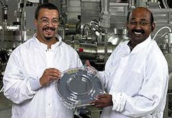
Motorola Labs (Tempe, AZ) made a big splash in the electronics world when it announced a new technique for fabricating gallium arsenide (GaAs) components on a silicon substrate. The likely immediate impact is to help cut the cost of GaAs components, but company officials say the long-term promise of the technology is in optoelectronics.
Cheap and easily made in large wafers, silicon would be an ideal substrate for III-V semiconductors, if their lattice constants matched. However, the lattice spacing in GaAs is 0.5653 nm, 4.1% larger than the 0.5431-nm lattice spacing in silicon. The lattice spacing in indium phosphide is even larger, about 0.588 nm. Epitaxial growth of thick layers of GaAs can accommodate the mismatch between GaAs and silicon, but the process is too expensive for mass production.
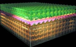
Motorola's new process takes a different approach, depositing a couple of microns of strontium titanate (SrTiO3 or STO) on the silicon. Oxygen penetrates the crystalline SrTiO3, producing an amorphous layer in contact with the silicon, which can accommodate the lattice mismatch. Then GaAs can be grown on top without producing the defects that form when it is grown directly on silicon. Just looking at voltage-current curves, "we could not tell GaAs on silicon from GaAs on a GaAs substrate," says Jim Prendergast, vice president and director of the physical sciences research laboratory at Motorola Labs.The new process can make GaAs-on-silicon components at lower cost than GaAs on GaAs substrates, says Tom Hierl, chief technology officer at IQE (Bethleham, PA), which is developing equipment and materials for the process. Motorola has filed more than 270 patent applications, and plans to license its technology broadly. Motorola has demonstrated GaAs LEDs made on silicon substrates and Prendergast says lasers will be a focus for future research. So is another crucial factor for optoelectronics—the ability to make optical and electronic connections between the two materials. Developers would like to integrate GaAs optical components with silicon electronics to make inexpensive fiberoptic transmitters and receivers for such applications as local-area networks and fiber to the home. Motorola is working on such components, but they are more challenging, says Joachim Piprek of the University of California at Santa Barbara. The university has fused indium phosphide (InP) and GaAs chips to make VCSELs in which light and current pass through the interface, but still is trying to reduce defect levels.
In the long run, Motorola hopes to extend its process to InP, the substrate for 1.3- and 1.55-µm fiberoptic light sources, as well as a material that can produce very fast electronics. The lattice mismatch between InP and silicon is more than 8%, so Motorola is looking at related oxides that might serve as interface layers. The company isn't ready to talk about the details. Motorola also is looking at gallium nitride compounds and thinking of making blue lasers on silicon substrates, says Prendergast. "We really believe this is a broad approach; the first application happens to be GaAs."
About the Author
Jeff Hecht
Contributing Editor
Jeff Hecht is a regular contributing editor to Laser Focus World and has been covering the laser industry for 35 years. A prolific book author, Jeff's published works include “Understanding Fiber Optics,” “Understanding Lasers,” “The Laser Guidebook,” and “Beam Weapons: The Next Arms Race.” He also has written books on the histories of lasers and fiber optics, including “City of Light: The Story of Fiber Optics,” and “Beam: The Race to Make the Laser.” Find out more at jeffhecht.com.

