Particle Accelerators: Laser-based microchip electron accelerator can benefit industry and medicine
If electron accelerators could be made small and cheap enough, not only would every university be able to afford its own accelerator laboratory, but inexpensive coherent x-ray beam sources for photolithographic processes in the semiconductor industry could be made available, which could reduce transistor size in computer processors and increase integration density. For medical use, accelerator-based endoscopes could be used to irradiate tumors deep within the body with electrons.
The Accelerator on a Chip International Program (AChIP), funded by the Gordon and Betty Moore Foundation in the U.S., aims to create an electron accelerator on a silicon chip. The fundamental idea is to replace accelerator parts made of metal with glass or silicon, and to use a laser instead of a microwave generator as an energy source.
Because of glass’s higher electric-field load capacity, the acceleration rate can be increased and thus the same amount of energy can be transmitted to the particles within a shorter space, making the accelerator shorter by about a factor of 10 than traditional accelerators delivering the same energy.
One of the challenges is that the vacuum channel for the electrons on a chip has to be made very small, which requires that the electron beam be extremely focused. Because the magnetic focusing channels used in conventional accelerators are much too weak for this, a new focusing method must be developed if the accelerator on a chip is to become reality.
2D design enables photolithographic fabrication
Researchers at Technische Universität (TU) Darmstadt, led by researcher Uwe Niedermayer, are now using the laser’s electromagnetic field itself to focus electrons within a channel only 420 nm wide.1 The concept is based on abrupt changes to the phase of the electrons relative to the laser, resulting in alternating focusing and defocusing in the two directions in the plane of the chip surface. This creates stability in both directions.
Perpendicular to the chip’s surface, weaker focusing is sufficient, and a single quadrupole magnet encompassing the entire chip can be used. This concept is similar to that of a conventional linear accelerator. However, for an accelerator on a chip, the electron dynamics have been changed to create a two-dimensional (2D) design that can be realized using lithographic techniques from the semiconductor industry.
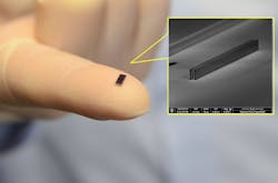
The device consists of a photolithographically fabricated standing-wave dual-pillar structure irradiated by z-polarized laser pulses with a 2 µm wavelength and 100 fs duration incident from both sides of the structure, which is about 5 mm long (see figure). The incident lasers’ field strength from both sides is 187 MeV/m and 500 MV/m. The structure keeps the accelerated electron beam focused along the entire 5 mm length of the accelerator to within ±0.21 µm. The full-width at half-maximum (FWHM) of the resulting electron pulse is 0.11 fs in duration.
Niedermayer is currently a visiting scientist at Stanford University (Palo Alto, CA), which is leading the AChIP program along with the University of Erlangen in Germany. At Stanford, Niedermayer is collaborating with other AChIP scientists with the aim of creating an accelerator on a chip in an experimental chamber the size of a shoebox. A commercially available system combined with nonlinear optics is used as a laser source. The aim of the AChIP program, which has funding until 2020, is to produce electrons with 1 MeV of energy from the chip. An additional aim is to create ultrashort (less than 10-15 s) electron pulses.
REFERENCE
1. U. Niedermayer et al., Phys. Rev. Lett. (2018); https://link.aps.org/doi/10.1103/physrevlett.121.214801.
About the Author
John Wallace
Senior Technical Editor (1998-2022)
John Wallace was with Laser Focus World for nearly 25 years, retiring in late June 2022. He obtained a bachelor's degree in mechanical engineering and physics at Rutgers University and a master's in optical engineering at the University of Rochester. Before becoming an editor, John worked as an engineer at RCA, Exxon, Eastman Kodak, and GCA Corporation.

