ZnO photonic-crystal laser emits in the UV
Although low-threshold lasing in the IR has been realized in photonic-crystal slabs made of III-V semiconductor materials, a UV photonic-crystal laser represents a special challenge because of the different materials and the smaller feature sizes required for the crystal. Although the small feature size is difficult to achieve in commonly used wide-bandgap materials such as gallium nitride (GaN) and zinc oxide (ZnO), demands for compact blue and UV light sources have prompted much research in this area. Building on a recent demonstration of photonic-crystal UV light-emitting diodes fabricated with III nitrides, a team of researchers from the Materials Research Center at Northwestern University (Evanston, IL) has demonstrated an optically pumped ZnO photonic-crystal laser operating in the near-UV at room temperature.
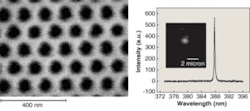
The photonic-crystal structure was prepared by growing 200-nm-thick ZnO films on c-plane sapphire substrates by plasma-enhanced metal-organic chemical-vapor deposition. Next, arrays of cylindrical columns were removed by focused-ion-beam (FIB) etching at 30 KeV (see figure). Structural damage caused by the FIB process was then removed by annealing the films in oxygen at 600°C for one hour. By adjusting the lattice constant a, and the radius of the air cylinders r, the ZnO gain spectrum can be made to overlap the photonic bandgap.
In the experimental setup, a 10×-microscope objective lens is used to focus a modelocked Nd:YAG laser (355‑nm wavelength, 10-Hz repetition rate, 20-ps pulse length) at room temperature to a 4-μm spot on the patterned ZnO film. A beamsplitter routes the emission through another lens and into a UV fiber connected to a spectrometer with 0.13-nm spectral resolution. Because the sapphire substrate is transparent in both visible and UV frequencies, a 20×-microscope objective lens is placed at the backside of the sample for measurement of the spatial distribution of emission intensity. The sample was also illuminated by a white-light source to identify the position of the lasing modes in the photonic lattice.
Although the ZnO-patterned films had structures with lattice constants a varying from 100 to 160 nm, only the patterns with a = 115 nm and 130 nm were able to lase. The spectral emission from a pattern with a = 115 nm andr/a = 0.25 was a single sharp peak at 387.7 nm with a spectral width of 0.24 nm above the lasing threshold. The near-field image of the lasing mode showed spatial localization to a small region approximately 1 µm in diameter inside the 8 × 8-μm patterned region of the film (see figure).
Calculation of the photonic band structures using a 3-D plane-wave-expansion method revealed a bandgap from 396 to 415 nm for the structure with a = 130 nm and a narrower gap from 363 to 372 nm for the structure with a = 115 nm. With the gain spectrum for ZnO ranging from 373 to 397 nm, the calculated photonic bandgaps for these two structures do not exactly overlap the gain spectrum. The team surmised that the unavoidable imperfections in the structures created during the fabrication process broadened the bandgaps and made them shallower, allowing overlap and lasing modes to occur on the lower-frequency side of the bandgap (near the dielectric band edge) for the a = 115 nm structure and on the higher-frequency side of the bandgap (near the air band edge) for the a = 130 nm structure. The lasing threshold of the structure with a = 115 nm is lower than that of the latter because the defect modes are concentrated inside ZnO and experience more gain.
The research team now understands that the lasing modes are basically spatially localized defect states near the edge of the photonic bandgap that are formed by structural disorders unintentionally introduced during the fabrication process. “It is very difficult to make the intentionally introduced defect modes repeatable, especially in the UV regime,” says researcher Hui Cao. For this reason, the team plans to focus on minimizing the structure disorder so that they can get lasing in intentionally introduced defect modes.
REFERENCE
X. Wu et al., Appl. Phys. Lett. 85, 17 (Oct. 25, 2004).

