Optoelectronics World News
Photonics West ’05 reflects more mature industry
From fiber lasers and high-power diode arrays to light-emitting diodes (LEDs), spectrometers, and biomedical imaging, Photonics West 2005 (Jan. 22-27; San Jose, CA) featured hundreds of technical presentations and product demonstrations that not only captured the diversity of this industry but reflected a subtle shift toward more applications emphasis at this traditionally technology-oriented conference.
“There are so many emerging technologies and applications that it is a natural evolution for this industry and this conference to include more applications,” said Marilyn Gorsuch, SPIE event manager for Photonics West. “And given the structure of Photonics West (BiOS, OPTO, LASE, and MOEMS-MEMS), there is a lot of synergy and a lot of potential for cross-fertilization.”
But Photonics West is still a technologist’s paradise and still the leading event at which to launch new products and create new product-development and distribution relationships. According to SPIE, this year’s Photonics West was the organization’s most successful technical meeting and exhibition ever. The event drew a record 15,000-plus attendees and nearly 800 exhibiting companies. In addition, there were 2300 papers in 80 technical conferences covering the latest developments in lasers, optoelectronics, MEMS/MOEMS, imaging, and biomedical optics.
The show got off to a busy start with the annual Biomedical Optics (BiOS) conference, which also saw significant growth in its vendor exhibits- 90 companies showcased their components and instrumentation this year, up 30% from 2004. In addition, the annual Saturday night BiOS Hot Topics event was attended by a standing-room-only audience of nearly 500. The Hot Topics once again showcased the state of the art in biomedical research and applications, with particular emphasis on optical imaging and nano-based applications. Britton Chance, professor emeritus of biochemistry, biophysics, physical chemistry, and radiologic physics at the University of Pennsylvania (Philadelphia, PA), received a lifetime achievement award for his pioneering work in biomedical optics and presented results from a six-year study of breast-cancer identification using a low-cost, hand-held optical diffuse-scattering measurement technique (see Laser Focus World, February 2005, p. 24).
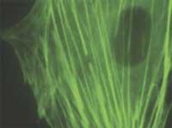
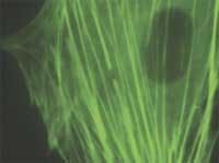
On the therapeutic side, Eric Mazur, professor of applied physics and physics at Harvard University (Cambridge, MA), gave a talk on cellular microsurgery using ultrashort laser pulses (see figure; also Laser Focus World, January 2004, p. 34). For the last 20 years, Mazur’s research group at Harvard has been studying the dynamics of molecules, chemical reactions, and condensed matter on very short timescales using laser pulses. This work has led to subcellular surgery and nanosurgery, where femtosecond laser pulses are used to selectively disrupt submicrometer-sized organelles within living cells or tissue without affecting the surrounding material or compromising viability of the cell or organism.
On the show floor
As in years past, a number of vendors used Photonics West as a platform for launching new products, new strategies, and new ideas. Leading the pack were the fiber-laser vendors.
“Fiber lasers can do anything solid-state lasers can do,” said R&D manager John Clowes from Fianium (Southampton, England), which displayed several fiber-laser products in its booth and presented information on new developments in compact, ultrafast fiber-laser sources that offer improved beam quality, small size, and low cost.
Among the new fiber-laser products introduced were:
SPI Optics (Southampton, England) announced the latest additions to its range of redPOWER fiber lasers and some unique beam-delivery optics that are back-reflection tolerant.
Nufern (East Granby, CT) unveiled a line of continuous-wave fiber-laser modules, the PumpGuard optical fiber for multimode diodes, a PANDA-style fiber for visible and near-IR wavelengths, and a thulium-doped double-clad fiber.
Aculight (Bothell, WA) premiered its new PF1550-36 pulsed fiber-laser (1.54 µm) for applications in laser range-finding, sensing, and micromachining.
Del Mar Ventures (San Diego, CA) introduced all-solid-state fiber lasers based on erbium-doped and ytterbium-doped nonlinear optical fibers.
Aside from fiber lasers, there were numerous other notable product introductions.
Hamamatsu (Bridgewater, NJ) released the S9376 series CCDs for fluorescence spectrometers and Raman spectrophotometers; the H9530 series of 8-channel linear array multianode photomultiplier-tube assemblies; silicon avalanche photodiodes with high resolution and performance in a 3.5 × 4.0-mm package; and large-area PIN photodiodes for direct detection of charged particles and x-rays.
Bookham (San Jose, CA) launched what it says is the world’s most powerful commercially available continuous-wave laser-diode bar, a 9xx-nm 120-W CW multimode system.
Newport (Irvine, CA) unveiled the SmartTable, an optical table that provides a 10 times improvement in reducing resonant structural vibrations and settling time, and minimizing vibration of components attached to the table surface.
Coherent (Santa Clara, CA) introduced new 940- and 980-nm fiber-coupled laser-diode bars with what the company says is the highest efficiency in the industry (greater than 50%).
Lambda Physik introduced its “Pro” series lasers that build on the existing COMPex and LPX excimer laser series (now called COMPexPro and LPXPro).
Polychromix (Wilmington, MA) revealed preliminary device specifications for a near-IR spectrometer that uses the company’s MEMS spatial-light modulator.
International flavor
Photonics West 2005 was also notable for the number of international exhibitors on the tradeshow floor. Germany alone was represented by some 70 companies, and Scotland, Wales, the U.K., and France all set up dedicated pavilions to showcase several of their young and growing photonics companies.
OSRAM Opto Semiconductors (Regensburg, Germany) showcased the OSRAM Sirilas SPL LG81, for solid-state pumping, material processing, illumination and industrial applications; OSTAR, a compact, high-power LED designed for miniature projection, head-up automotive displays, and industrial applications; and the Golden DRAGON LED, a 2-W LED that provides brighter light in a low thermal-resistance package.
Mesophotonics (Southampton, England) released its Klarite substrates for surface-enhanced Raman spectroscopy (SERS; see “Nanopatterned substrates target Raman spectroscopy,” p. 38).
Varioptic (Lyon, France) displayed its electrowetting-based liquid lens that is being targeted for zoom and autofocus usage for camera cell phones (see Laser Focus World, November 2003, p. 17). The low-cost technology comprises a water/oil mixture that deforms into a lens shape with application of electrical current.
Kathy Kincade
Flip-chip imager achieves 300-nm resolution
Researchers at Heriot-Watt University (Edinburgh, Scotland) have combined two-photon excitation with solid-immersion-lens (SIL) imaging to achieve a lateral resolution of 325 nm in subsurface imaging of a silicon flip chip. The achievement is part of an ongoing project to develop optical metrology methods to support continued progress on the International Technology Roadmap for Semiconductors (ITRS; a study cosponsored by numerous semiconductor industry associations worldwide).1, 2
The ITRS forecasts 45-nm feature sizes by 2010 and also notes a need for nondestructive wafer- and mask-level microscopy for measuring critical dimensions and detecting defects. Optical technologies, as opposed to electron- or ion-beam technologies, for instance, offer a number of advantages for these tasks such as the ability to operate in air, no associated charge buildup, an ability to probe areas that are inaccessible to contact probes, and high-speed sampling without parasitic capacitance. But optical technologies are also limited in resolution by the wavelength of light.
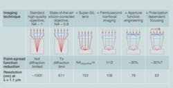
The smallest separation of two points (∆x) that can be distinctly imaged has been described using the equation ∆x = 0.5λ/NA, where NA is the numerical aperture of the imaging system, according to Derryck Reid, who leads the ultrafast-optics group at Heriot-Watt University. “The best conventional microscopes achieve NA approximately equal to 1 and the resolution limit in silicon is therefore on the order of 600 nm,” he said. “Our project aims to improve this figure by up to a factor of 10 by combining novel SIL techniques with confocal, nonlinear, and other resolution-enhancing strategies never before applied to this problem.”
Flip-chip difficult to look into
In describing the problem that they are attempting to solve, Reid pointed out that, while the topology of flip-chip semiconductor circuitry enables high circuit density by taking advantage of multiple levels, it also eliminates traditional optical and mechanical routes for subsequent metrology. Conventional subsurface integrated-circuit imaging uses 1064-nm laser-confocal microscopy to image through the silicon substrate; state-of-the-art technology can approach the diffraction limit, he said. But the conventional process requires major tradeoffs between signal level, image contrast, and penetration depth, he said.
Substrates must be thinned prior to imaging because of silicon’s high absorption coefficient at 1064 nm, and even after thinning only 20% of the light manages to penetrate a 200-µm-thick substrate. So the prospect of further improving resolution by boosting the NA with several additional millimeters of silicon in the form of a silicon immersion lens is problematic at this wavelength. Reid’s team has gotten around the problem of silicon absorption, however, by using 400-fs pulses of 1530-nm light from an erbium fiber laser to get well above the silicon band edge and to excite two-photon absorption and stimulate a measurable photocurrent at the beam focus within the sample.
Their solid-immersion lens (designed for maximum NA imaging of a flip chip with a polished silicon substrate, 0.35-µm feature sizes, and 100-µm thickness) had a radius of 2 mm and a depth of 2.47 mm, and was used with a 0.55-NA objective. In addition to achieving lateral resolution on the order of 300 nm, in future work the researchers expect to be able to perform sensitive depth measurements by detecting a change in signal when the focal plane is moved by only a few nanometers. The technique is more akin to profilometry than imaging, Reid said, but it may eventually provide noninvasive optical sectioning through devices such as vertical-cavity surface-emitting lasers.
Perfect flatness of the substrate to eliminate any gaps between the SIL and the chip-which the researcher did not have in the published experiment-will be required for the technique to actually achieve diffraction-limited performance, Reid added. The team also intends to improve resolution by working with laser wavelengths closer to the silicon bandgap, on the order of 1100 nm. Techniques under investigation to further improve resolution include a form of aperture-function engineering that provides narrower beam diameters (full width at half maximum) at the expense of larger side lobes, but then uses imaging techniques to suppress the side lobes; and polarization-dependent focusing based on tighter focusing in the s-direction than the p-direction because off-axis s-rays tend to be more strongly reflected at a dielectric interface.
Hassaun A. Jones-Bey
REFERENCES
1. E. Ramsay et al., Optics Lett. 30(1), 26 (Jan. 1, 2005).
2. E. Ramsay et al., Appl. Phys. Lett. 81(1), 7 (July 1, 2002).
Corrections
In Laser Marketplace 2005 Part I (January, p. 83) the numbers for solid-state lamp-pumped lasers for instrumentation in Table 1 and Table 2 were incorrect. The correct numbers are 295 (units) and 6,050 ($ thousands).
In Laser Marketplace 2005 Part II (February, p. 69) the last column on the individual market-segment tables were labeled incorrectly, the column heads should have said 2005.
SPECTROMETRY
null
Near-IR measurements monitor volcano activity
Changes in the gases emitted by active volcanoes indicate changes within the volcanoes, and can even warn of impending eruption. One of the main gases released by active volcanoes is carbon dioxide (CO2), whose two predominant isotopic forms are 13CO2 and 12CO2. “A small change of the 13CO2/12CO2 ratio-on the order of one part per million-can be due to magma movements toward the surface,” says Livio Gianfrani, an associate professor in experimental physics at the Seconda Università di Napoli (Caserta, Italy).
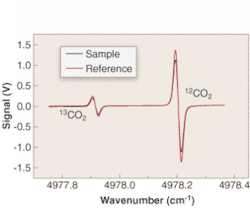
Gianfrani and his group have developed a laser diode-based portable spectrometer for measuring the CO2 isotope ratio and have tested it inside the Solfatara crater (north of Naples), which contains several hot gas-emitting fumaroles.1 The near-IR instrument has at its heart a room-temperature laser diode that emits at around 2 µm and is slightly tunable. The laser frequency is periodically scanned between 4977.5 cm-1 (2.0090 µm) and 4978.5 cm-1 (2.0086 µm) to enter in resonance with the 12CO2 R(17) and 13CO2 P(16) vibrational lines, at a rate of 0.2 Hz, explains Gianfrani. Absorption by the gas converts frequency modulation into amplitude modulation, giving raise to modulated signals at the modulation frequency and its integer-multiple values, whose magnitudes are proportional to the optical gas absorbance.
The group has brought the technology through more than one stage. Both the previous and current versions of the instrument contain a pair of gas cells to simultaneously and very precisely probe the 13CO2 and 12CO2 absorption lines in a sample gas cell as well as in a reference cell. In both cases, a single-mode room-temperature distributed-feedback laser diode emitting at 3 mW is used. In each cell, absorption of near-IR radiation is selectively and sensitively monitored using wavelength-modulation spectroscopy.
Single photodiode
In the new spectrometer, however, the two transmitted beams are monitored by a single thermoelectrically cooled preamplified indium gallium arsenide photodiode, says Gianfrani. To make this possible, a pair of electronic shutters alternately blocks each of the two beams, allowing only one beam at a time to be active. “This sequential approach offers the advantage of avoiding possible systematic deviations arising from the otherwise simultaneous use of two independent detection channels,” says Gianfrani. “Indeed, when using two photodiodes as in the earlier version, small but different nonlinear components of the responsitivity could influence the spectroscopic determination of the isotope ratio.”
The instrument is built on a 60 × 60-cm breadboard that is enclosed in a thermally insulating box (see figure). Volcanic CO2 is sampled by a gas dryer and cooler that produces water-free gas with a CO2 content of about 98%. The gas can be collected either in an evacuated flask for measurement at a later time, or via a 20-m-long tube to the spectrometer for measurement in real time at a flow of a few liters per minute. While off-line measurement was slightly more accurate, real-time measurement provided the obvious benefit of continuity. Slight nonlinearities introduced by the slightly differing molecular densities in the sample and reference gas cells could be calculated very precisely from the so-called Lambert-Beer law, and thus accounted for.
The field test showed single-measurement reproducibility and accuracy sufficiently good to allow tracking of changes in the CO2-isotope ratio. The instrument’s performance was compared to that of an isotope-ratio mass spectrometer (IRMS; a standard measurement tool). The data from off-line measurements of the laser-diode spectrometer agreed with data from the IRMS to absolute residuals ranging from 0.07 to 0.53 parts per thousand and a root-mean-square deviation of 0.3 parts per thousand. Real-time measurements agreed to a one-sigma uncertainty of 0.2 to 0.6 parts per thousand.
With a longer optical-absorption path length and choice of a proper spectral window, the technique could be extended to measuring the two oxygen (O) isotope ratios 18O/16O and 17O/16O, allowing the monitoring of volcanoes that produce less CO2. The researchers are planning other field campaigns in other volcanic areas, including Colli Albani (near Rome), says Gianfrani.
John Wallace
REFERENCE
1. A. Castrillo et al., Optics Express 12(26) 27 (December 2004).
NONLINEAR OPTICS
Time-prism pair creates fast optical delay
Important to applications in optical-coherence tomography, optical metrology, interferometry, and telecommunications, optical-delay lines have been developed using grating-based dispersive optics and scanning mirrors to obtain scanning rates on the order of 1 kHz, or by using acousto-optic modulators to achieve 1-MHz scanning rates. However, by using a time-prism pair, scientists from the School of Applied and Engineering Physics at Cornell University (Ithaca, NY) have demonstrated an all-fiber, programmable, ultrafast optical-delay line with a record scanning rate of 0.5 GHz and a range of 19 ps.1
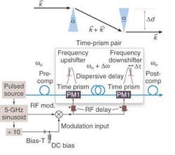
- A time-prism pair consisting of two lithium niobate (LiNbO 3) phase modulators is used to generate a time delay through frequency conversion and subsequent dispersive delay, provided by optical fiber. The time prisms are modulated by a 5-GHz sinusoid whose amplitude is modulated by the modulation input to the RF modulator. The time-prism pair is analogous to a spatial-prism pair (top), in that a shift in time is created for a pulse much like a shift in space is created for a light beam.
Lithium niobate frequency converters
The time-prism pair used by the Cornell scientists consists of a sinusoidally driven lithium niobate (LiNbO3) phase modulator as the first time prism, followed by a length of dispersive optical fiber. Tuning the drive voltage of this time prism changes the phase slope, inducing a wavelength shift due to phase modulation and a corresponding delay. To convert the frequency of the optical field back to its original value, another LiNbO3 phase modulator driven with the same sinusoid but π out of phase is used as the second time prism. Although frequency conversion with electro-optic phase modulation is not a new technique, this is the first time it has been applied to a rapid-scanning delay line.
In the experimental setup, a pulsed source emits an 8.0-ps, 5-GHz pulse train generated by pulse carving and time-lens compression (see figure). Pulses are upshifted in frequency by the first time prism, a sinusoidally driven LiNbO3 phase modulator. A time delay is introduced by 0.7 km of dispersion-compensating fiber with a total dispersion value of -74 ps/nm. The second time prism downshifts the frequencies back to their original values. Dispersion pre- and post-compensation of 37 ps/nm eliminates the pulse-broadening effects caused by the dispersive delay. To vary the frequency shift and the corresponding delay, the drive voltage of the phase modulators is adjusted through a broadband radio-frequency (RF) modulator, allowing programmable time delays.
To demonstrate the programmable delay, the scientists modulated the 5-GHz RF input with direct-current voltages. At the highest RF output into the phase modulator (4.24 Vπ), a frequency shift of 32.5 GHz is achieved, which resulted in a time delay of 19 ps. To demonstrate the rapid scanning capability of the delay line, the RF input was modulated with a 0.5-GHz sinusoidal waveform. Although the 0.5-GHz scanning rate over a 19-ps delay range is a record, the scientists can improve the delay range to 28 ps by introducing an improved drive waveform into the phase modulators. Through computer modeling, addition of a “correction” time prism (analogous to aberration correction in a time-lens system) can reduce nonlinearities in the phase-modulation drive and further reduce pulse distortions that limit the overall delay range.
Additional improvements to the system include replacing the fiber spools with other dispersive devices such as fiber Bragg gratings that could make the system more compact and reduce temperature variations and long fiber lengths that result in time-delay fluctuations. Further work has shown enhanced performance by using soliton propagation between time prisms which produces time delay without the adverse effect of dispersive pulse broadening and completely eliminates the need for pre- and post-dispersion compensation.2 Because scanning is not limited to the 0.5-GHz sinusoidal drive used in this experiment, but can consist of any desired RF waveform, the demonstrated ultrafast delay line permits electronically programmable pulse position, delay range, and scan rate.
“Who knows what temporal optical devices can be developed simply by borrowing concepts from the spatial-imaging domain, or vice-versa,” says James van Howe, one of the researchers.
Gail Overton
REFERENCES
1. J. van Howe and Chris Xu, Optics Lett. 30(1) 99 (Jan. 1, 2005).
2. J. van Howe and C. Xu, to be presented at OFC 2005, Anaheim, CA (March 6-11, 2005).
LITHOGRAPHY
Exactly resonant light mask controls atoms
Microstructured deposition of atoms controlled by a standing light field was first shown in 1992.1 Possible applications in lithography were immediately recognized. In the technique, an atomic beam is sent on its way to a substrate, but first passes through a planar near-resonant standing light field produced by counterpropagating monochromatic polarized light. Atoms that cross the field are affected by an intensity pattern with a spatial period of a half wavelength. The light field induces atomic dipoles so that the intensity pattern transforms into an optical potential pattern, focusing the atom flux and depositing it on the substrate in a periodic pattern. By using mirrors to generate standing waves, periodic patterns can be formed, for example, as parallel ridges and valleys (1-D), islands and depressions (2-D), or even 3-D volume gratings, with a minimum fundamental peak-to-peak distance of λ/2.2
Classical and quantum viewpoints
From the viewpoint of classical physics, near-resonant radiation induces atomic dipoles that oscillate with the driving field so that the time average of the potential energy of the dipoles in the field does not vanish, but instead amounts to a finite positive or negative value, depending on the sign of the frequency detuning from resonance. The strength of the atomic dipole is inversely proportional to the detuning and directly proportional to the electric field so that the potential energy follows the square of the effective field strength (that is, the intensity), enhanced by the inverse detuning. In case of resonance, in the classical description the induced dipoles oscillate phase-shifted by π/2 with respect to the driving field, resulting in zero time-averaged optical potential.
Atoms entering into a potential saddle at different lateral positions start to oscillate transversely, crossing the center line after having traveled a quarter of the oscillation period. That distance is the focal length of the atom-focusing lens. Atoms can be collected on a target behind intensity maxima if the laser is detuned to the blue from resonance, and behind the minima (due to sign reversal) for red detuning. By switching the detuning, λ/4 structures can be realized. Generally, an atom in a blue-detuned field can lower its energy by moving to lower light intensities, and vice versa for atoms in red-detuned fields. The focal length is proportional to the square root of the detuning and to the inverse square root of the intensity.
The classical picture does not explain other features, however. A quantum-mechanical description takes into account details such as magnetic sublevels of atoms, and allows calculations of potentials and forces obtained in more complicated field configurations that allow λ/4 and even λ/8 structuring. A convenient field configuration consists of two counterpropagating waves linearly polarized at 90° to each other. This configuration does not show spatially varying intensity, but instead shows spatially varying polarization from right- to left-handed polarization via intermediate linear polarization on a distance of λ/4. This results in a correspondingly spatially modulated optical potential for atoms with magnetic substates, such as chromium.
Exact resonance
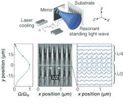
Now, researchers at the universities of Konstanz and Heidelberg, Germany, have tackled the exactly resonant case using a laser-cooled chromium atomic beam and a linearly polarized Gaussian standing light wave at 425.6 nm, resonant with the 7S3→7P4 transition (see figure).3 The laser power was 17 mW. The atoms crossed the laser beam near its waist so that the interaction time was limited to about the radiative lifetime of the excited state, thus avoiding dephasing by spontaneous emission. The resulting structure reveals the response for various intensities across the beam.
The structure shows a bifurcation at about half intensity, leading to λ/4 periods at lower intensities. At full intensity, λ/2 periods are obtained, as in the case of off-resonance fields. Solving the Schrödinger equation in momentum space, the authors succeeded in quantitative agreement with the experimental findings, even in details such as the scattering force due to spontaneous emission. The appearance of a λ/2 period at higher intensity and λ/4 at lower could be explained by taking into account intensity-dependent nonadiabatic transitions between the optical potentials displaced by λ/4 to each other. Hence, on-resonance interaction offers a new way for structured atom deposition with periods below λ/2. The perfect agreement encourages modeling of plane light masks generated by more than two beams. Three-dimensional structures could be made by evaporating two substances, one of which is in or near resonance for focusing, and the other is deposited in an unfocused manner as a matrix.4
Whether these results are important for semiconductor lithography remains unanswered. The results are highly important for atomic optics, however-a field of growing interest.
Uwe Brinkmann
REFERENCES
1. G. Timp et al., Phys. Rev. Lett. 69, 1636 (1992).
2. For a topical review see M.K. Oberthaler and T. Pfau, J. Phys. Condens. Matter 15, R233 (2003).
3. D. Jürgens et al., Phys. Rev. Lett. 93, 237402 (2004).
4. T. Müther et al., Microelectronic Eng. 57, 857 (2001).
FLAT-PANEL DISPLAYS
Flexible, transparent transistors made from amorphous-oxide semiconductors
Already used in microelectronics products such as flat-panel displays, thin-film transistors (TFTs), when combined with transparent circuit technology, could be used for display functions on transparent windows in cars or aircraft. The secret to further proliferation of TFTs in commercial and industrial display applications is lower-temperature, larger-area, and more-affordable fabrication techniques.
Although flexible solar cells and TFTs have been fabricated from organic semiconductors and hydrogenated amorphous silicon, silicon-based devices are not transparent because of their small bandgap and are limited in performance because of their low field-effect mobilities, typically on the order of 1 to 2.7 cm2V-1s-1. But researchers from the Frontier Collaborative Research Center and the Materials and Structures Laboratory of the Tokyo Institute of Technology (Yokohama, Japan) have recently fabricated transparent, flexible TFTs using amorphous oxide semiconductors with field-effect mobilities of 6 to 9 cm2V-1s-1.1 “We have explored amorphous-oxide semiconductors since 1994 and reported a series of novel materials. These materials have high performance comparable to those in crystalline ones and can be deposited at room temperature,” says researcher Hideo Hosono.
Optically transparent film
Films of transparent amorphous indium gallium zinc oxide (a-IGZO) were first prepared by pulsed-laser deposition with a krypton-fluorine excimer laser using a polycrystalline IGZO target at room temperature, for the purpose of determining the optical properties of the film. X-ray diffraction of the a-IGZO film on the glass substrate showed that the film was optically transparent in the entire visible and near-IR regions from 390 to 3200 nm, with an optical transmittance better than 80% and thermal stability up to 500°C in air.
Next, the team fabricated flexible, transparent TFTs using the a-IGZO film as an n-channel active layer on 200-µm-thick polyethylene terephthalate (PET) films. Standard photolithography and lift-off techniques were used for the source, drain, and gate contacts and the gate insulator. The layers were deposited by pulsed-laser deposition at room temperature using yttriumoxide (Y2O3) and indium tin oxide (ITO) ceramic targets. The channel length and width were 50 and 200 µm, respectively. Film thicknesses for the a-IGZO active layer, the Y2O3gate, and the ITO electrode were 30, 140, and 40 nm, respectively. Measurements in air and at room temperature show typical source-to-drain current and voltage characteristics of a TFT. The estimated saturation mobility of the fabricated sample was approximately 8.3 cm2V-1s-1, which is much larger than the values obtained for organic and hydrogenated amorphous silicon. In addition, a low off-current on the order of 10-7 A and an on-to-off current ratio of approximately 103 were obtained.
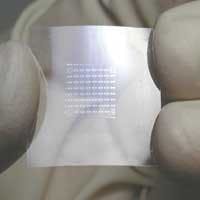
To demonstrate flexibility, the team next examined bending effects on the transparent TFTs (see figure). After initial bending into a curve with a radius of curvature of 30 mm (corresponding to a tensile strain of approximately 3%), the transparent TFTs maintained good characteristics, although a slight decrease was observed in the saturation current. Even after repetitive bending, the device characteristics were reproducible and stable at temperatures up to 120°C. The devices are inoperative at temperatures higher than this, however, most likely due to the softening of the PET substrate. For the research team, these promising characteristics imply that transparent amorphous-oxide semiconductors have the potential to overtake hydrogenated amorphous silicon for applications in transparent, flexible displays.
Gail Overton
REFERENCE
1. K. Nomura et al., Nature 432, 488 (Nov. 25, 2004).
FLAT-PANEL DISPLAYS
Electrowetting and lumophores make bright pixels
The phenomenon of electrowetting, in which an applied electric field changes the contact angle of fluids against a hydrophobic surface, has been used in fluidic optical devices such as variable-focus lenses (see Laser Focus World, November 2003, p. 17). Often, two immiscible fluids are used, with the interface between them experiencing the adjustable angular shift. In a development that exploits electrowetting and fluorescence, researchers at Extreme Photonix (Cincinnati, OH) and the Nanoelectronics Laboratory at the University of Cincinnati (Cincinnati, OH) have developed a switchable light-wave-coupled (LWC) device that can serve as pixels for a bright flat-panel display.
The first prototype consists of a 15 × 30 array of pixels, each 1 × 3 mm in size, on a glass substrate that serves as the conduit for the excitation light. To make the device, a transparent indium tin oxide electrode and a solid hydrophobic insulating layer are deposited on glass, followed by solid hydrophobic cladding elements that cover part of each pixel and a solid hydrophilic grid that defines the pixel boundaries. A water layer is spread over the array and second electrodes placed in the water near an edge of each pixel. In the final step, a layer of fluorescent oil a few tens of microns thick is inserted into each pixel, coating each pixel and taking up residence between the water layer and the hydrophobic insulating layer.
Nonpolar lumophores
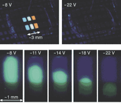
Lensed violet (405 nm) gallium nitride-based light-emitting diodes are optically coupled into one edge of the glass substrate, which has a refractive index of 1.46. Mixed into the oil is approximately 1% (by weight) of a red, blue, or green nonpolar organic fluorescent lumophore. When a voltage is applied, the oil layer bunches up and moves to one side of the pixel, baring the glass to the water (which has a refractive index of 1.33); switching off the voltage causes the oil to form again as a layer.
When the oil layer is absent (voltage on), the angularly incident violet light is confined by total internal reflection (TIR) to the substrate. When the oil layer is present (voltage off), the violet light spreads into the oil, causing its lumophore to fluoresce with a quantum efficiency of approximately 90%, and is reflected by TIR at the oil/water boundary back into the glass (see figure). In the absence of the lumophore, the violet light is hardly visible because the eye has a low photopic response at that wavelength; even so, a low-cost filter coating can be added to block violet light (the coating would serve the more important function of blocking ambient light from exciting the lumophores-crucial for sunlight-viewable displays).
The 1 × 3-mm pixels in the first device have a switching time of 100 ms or less, a luminance of up to 500 cd/m2, and a contrast ratio of 20:1. The prototype works well in any orientation. “With proper design, gravity, vibration, and orientation is a nonissue,” says Jason Heikenfeld, one of the researchers. “Proper design simply requires that you use polar and nonpolar liquids with equal densities and provide a top plate to seal the liquid system. We have developed several density-matched liquid systems.”
Fast switching
The size of the 1 × 3-mm pixel was chosen simply for ease of experimentation; the researchers have tested smaller devices with dimensions of several hundred microns. “Electrowetting requires mass (liquid) acceleration; the on/off switching time actually improves as you decrease size,” says Heikenfeld. “Typically, one can achieve less than 10-ms switching speeds for these devices. Electrowetting in general has the potential to provide switching speeds in excess of 1000 Hz, which is well beyond the approximately 100 Hz needed for applications such as video displays.”
Choice of materials is important, notes Heikenfeld. “For our specific electrowetting application, one of the main concerns is aging of the lumophores,” he says. “We have two very strong advantages to our lumophore system. First, we used nonpolar lumophores doped into nonpolar mediums that are nonreactive (unlike polar water-based dyes and systems, which degrade quickly). Second, we use a soft excitation source at 400 nm that decreases the amount of nonradiative energy the lumophores must absorb during visible photo generation. We have found that our lumophores actually outlast both the commercial LEDs and plasma lamps that can be used to pump them. This is not true of all lumophores. Through careful lumophore selection and design, we can achieve the tens-of-thousands-of-hours requirement for commercial applications. Use of a 400-nm source is also critical also because the optics used in the light-storage plate are highly transparent at this wavelength.”
The researchers are focusing on advancing the design and using materials that improve the contrast ratio to 100:1 or greater. “We also have some exciting work in electrowetting light valves that operate in a transmissive mode,” says Heikenfeld. “These use a white backlight, chromophores instead of lumophores, and are greater than 80% transmissive for light at any polarization or incidence angle.”
John Wallace
LASER COMMUNICATIONS
Supercontinuum multiplexing speeds free-space communications
Robert Alfano and Joseph Zeylikovich, scientists at the Institute for Ultrafast Spectroscopy and Lasers in the Department of Physics at the City College of the City University of New York (CCNY; New York, NY) have demonstrated multiplexing and ultrafast multichannel spatially resolved demultiplexing of supercontinuum (SC) coherence data packets using a coherent time-to-space conversion as an approach for free-space ultrafast laser communication. The advantage offered by an SC source in free-space and fiberoptic systems is its super-broadband spectrum for simultaneously generating more than 100 channels with fixed spectral spacing.
Supercontinuum pulses-ultrafast, broadband “white-light” pulses that can span a spectral region from the UV to the near-IR-arise from the nonlinear response of ultrashort pulses focused into a transparent medium. The SC light is highly coherent, meaning that its spectral phase is stable and does not change much from pulse to pulse.
In the approach demonstrated by the scientists, spatially encoded multichannel coherence multiplexing is used in addition to time-delay multiplexing. Shaping, signal processing, and time-space conversion of femtosecond pulses is achieved by linear and nonlinear manipulation of the spatially dispersed optical-frequency spectrum within a grating pair and lens pulse shaper. A coherent cross-correlation technique is used for the detection of the signal-pulse packets on a femtosecond time scale and requires a coherent replica of the broadband source at the receiver as a reference signal (which has passed through a physical medium identical to that traversed by the SC signal-data packets).
Single-shot detection
The proposed receiver does not have any moving parts and permits single-shot detection of all time-delayed data bits distributed in multiple spatially resolved channels. Multiple frequencies are generated by the interference of SC pulses separated by a segment of time. In addition, the SC pulses interfere with one another in the spectral domain. This interference generates many individual frequency channels in the supercontinuum spectrum that can then be used to transmit information. “In the optical spectrum, the pulses generate multiples of discrete optical-wavelength channels. In this way, we are able to create hundreds of new communication channels for applications,” says CCNY researcher Joseph Zeylikovich.
In the experimental setup to demonstrate the technique, a modelocked Ti:sapphire amplifier system centered at 800 nm provides 200-fs pulses with a repetition rate of 250 kHz and 20-MW peak power (see figure). The laser output is focused into a plane-parallel plate of heat-resistant glass rotated at 2 Hz to provide stable SC generation extending from 400 to 850 nm. The SC pulses are then split into two parts-a signal beam and a reference beam. The signal beam is directed into the coherence multiplexer, where the SC signals are imprinted on light via path-difference multiplexing. The signal and reference beams interfere at a diffraction grating and interference fringes are focused into a CCD array by a lens. A spatial filter at the focal plane of the lens selects the first-order diffraction from the respective beams, with the diffraction grating introducing a continuous optical delay along the dispersion direction.
A series of cross-correlation calculations on the intensity distribution measured by the CCD yield the autocorrelation function of the SC pulse, which allows for extraction of the optical information-data-packets envelope (essentially, the spatial and temporal representation of multiple channels separated by a particular frequency, depending on the original separation time of the SC pulses).
To date, the research team has produced as many as 60 frequency channels separated by 75 GHz for two SC pulses separated in time by 13.6 ps. The team is interested in licensing this technology for communications applications, and continues work on applying the supercontinuum to space, remote sensing, and military applications.
Gail Overton
REFERENCE
1. I. Zeylikovich and R. R. Alfano, IEEE J. Sel. Topics in Quant. Electron. 10(5) 1233 (September/October 2004).
Photonic Crystals
Nanopatterned substrates target Raman spectroscopy
Researchers at Mesophotonics (Southampton, England), a spinoff of the University of Southampton, have developed integrated, planar photonic-crystal technology that allows light to be bent, routed, and processed at a submillimeter scale. The technology has been commercially introduced; at Photonics West 2005, the company unveiled an application of its technology platform focused specifically on surface-enhanced Raman spectroscopy (SERS).
The Mesophotonics technology is based on planar-waveguiding photonic crystals made of CMOS-compatible silicon materials. This approach allows the fabrication of optical manipulation, optical-signal processing, and electronic circuitry on single substrates using standard silicon-foundry processes. The planar photonic crystals are fabricated using standard lithographic techniques.
The function of any particular planar photonic crystal is determined entirely by the geometry of the lattice of air holes, according to the company, which lists switches, splitters, combiners, prisms, wavelength multiplexers, delay lines, filters, polarization controllers, mirrors, cavities, feedback devices, beam shapers, gain-modification devices, and dispersion controllers among the potential devices and applications.
Integrated circuits based on this technology platform could conceivably perform several functions, each defined by the distribution of air holes and connected to each other by planar optical waveguides. The interconnection scheme would be analogous to the integration of electronic circuitry, but the actual device fabrication is envisaged as being much simpler, with all devices perhaps being fabricated in one mask step in which a single air-hole pattern defines all of the devices and interconnections, as well as the functionality of the entire circuit.
As initial steps toward the realization of this ambitious goal, the company introduced a continuum-generation chip (CGC) last year, and a so-called Klarite substrate for SERS this year at Photonics West. The latest generation of CGC integrates 40 polarization-preserving 2-D planar waveguides of differing sizes on a 1-cm chip, effectively enabling investigation of changing waveguide geometry without changing the sample. The company’s SERS substrates are based on nanometer-scale patterning of a gold surface, such that the photonic crystal controls the surface plasmons that govern the SERS amplification. The SERS substrates are mounted on 75 × 25-mm microscope glass slides compatible with most micro-Raman spectrometers.
The signals generated from the SERS substrates are orders of magnitude more intense than traditional Raman signals and enable detection with low-sensitivity detectors and low-power lasers, which will open the door to the development of low-cost Raman detection systems compatible with volume OEM applications, according to John Lincoln, business-development director at Mesophotonics.
“We believe that Klarite substrates offer a new method of controlling surface-enhanced Raman amplification that provides the reproducibility necessary for a vast range of detection applications,” he said.
Hassaun A. Jones-Bey
FIBEROPTIC GYROSCOPES
Frequency-modulated interference increases fiber-gyroscope sensitivity
Although various techniques have improved the performance of fiberoptic gyroscopes (FOGs) in recent years, a variation of an existing technique has been demonstrated that solves the problems of a zero-sensitivity point (when the rotation speed approaches zero, the sensitivity approaches zero), ambiguous determination of rotation direction, inaccurate calibration, and ambiguous fringe count, and greatly improves resolution.
Frequency-modulated continuous-wave (FMCW) interference analysis was first developed for fiberoptic gyroscopes by Culshaw and Giles in 1982.1 In their setup, two independent Mach-Zehnder interferometers were used to sense the rotation velocity. Because a fiber coil was used as one arm of the interferometer, the length of the fiber coil depended on the coherence length of the light source (typically a few meters), thus limiting the length of the coil and reducing resolution.
Now, Jesse Zheng at PhotonTech (Vancouver, BC, Canada) has applied FMCW in a new way. In Zheng’s approach, a fiber-coupled laser-diode source is coupled into a series of four fiberoptic directional couplers to constitute an unbalanced fiberoptic Sagnac interferometer-unbalanced in the sense that the two optical arms of the interferometer are not equal in optical path length.2 The polarized, frequency-modulated laser beam is divided into two beams by the first directional coupler, FC1 (see figure). One beam passes through FC2 and enters the upper end of the fiber coil, while the other passes through FC4 and enters the lower end of the fiber coil. These two beams propagate in opposite directions, pass through couplers FC4 and FC2 again separately, and enter fiber coupler FC3 to mix coherently. The beat signal that is produced exits from FC3 and is received by the photodiode.
Because the fiber coil can be as long as a few kilometers because of the nature of the Sagnac structure, the resolution of the gyroscope is improved by at least a factor of 100. In addition, the rotation velocity is determined by measuring the phase shift rather than the beat frequency, improving resolution by thousands of times.
Zheng used a laser diode with a 661.6-nm wavelength and a continuous power rating of 5 mW, modulated at 10 kHz with a sawtooth waveform. The detector was a silicon p-i-n photodiode with a 1-ns rise time; the single-mode fiber coil was 0.1 m in radius and 100 m in length. To determine the phase difference with respect to a standard reference signal (derived from the ramp modulation input), the most intense harmonic component (4 × 10 kHz) in the signal was chosen. The experimental resolution was 0.02°/s.
The gyroscope is limited mainly by the variation of the initial optical-path difference between the two interfering beams, in which the fibers linking the directional couplers can introduce an undesired nonreciprocal phase drift due to temperature changes. To eliminate these limitations, Zheng suggests that a temperature-control system should be implemented. If not, and if the fiberoptic network is properly designed, the nonreciprocal phase drift could be compensated either optically or electrically. “Considering its multiple advantages (dynamic signal, fully passive, compact, and light), the fiberoptic FMCW gyroscope could be the next generation for fiberoptic gyroscopes,” Zheng says.
Gail Overton
REFERENCE
1. B. Culshaw and I. P. Giles, IEEE J. Quant. Electronics QE-18, 690 (1982).
2. J. Zheng, Optics Lett. 30(1) 17 (Jan. 1, 2005).
