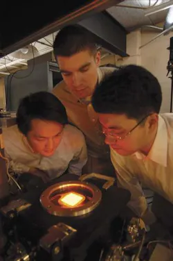
A group at the University of Illinois (Urbana, IL) developing microdischarge arrays (see Laser Focus World, March 2002, p. 9) has now produced versions that contain up to 40,000 pixels that are scalable to even higher pixel counts.1 The devices, which are created lithographically on silicon wafers, contain arrays of cavities typically on the order of 50 to 100 µm in size that are filled with neon or another gas at near or greater than atmospheric pressure. Alternating-current (AC) excitation of the gas through microelectrodes at a few hundred volts and frequencies of 5 to 20 kHz produces strong emission at UV and visible wavelengths.
The most obvious use for the devices is in flat-panel displays. A microcavity-plasma display would be quite different from a conventional TV-type plasma-display panel (PDP). While a PDP has pixel sizes on the order of a millimeter, the pixels in a microdischarge array can approach 10 µm in size. And because microdischarge arrays are fabricated monolithically in silicon, they are potentially easier to produce in high volume. The devices’ high UV output makes them suitable for nondisplay applications, too.Good uniformity, few defects
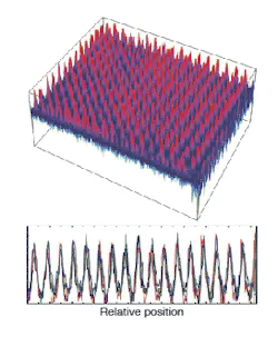
The researchers fabricated several 200 × 200-pixel arrays with 100‑µm periods; the substrates for the 20 × 20-mm devices were 2-in.-diameter silicon wafers. A typical array excited at a frequency of 10 kHz draws about 30 mA of current. The pixel-to-pixel uniformity is reproducible and uniform to within ±10% over the entire array. Though fabricated under nonoptimum conditions in a multi-user facility, the arrays had ten or fewer defective pixels per array, all resulting from thickness variations in one of the device’s several thin-film coatings (silicon nitride).
"We believe that the small pixel size will enable us to make high-resolution displays,” says Sung-Jin Park, one of the researchers. “The microcavity-plasma device has a vertically formed electrode system, not the parallel sustain electrode system as in PDPs, so we can change the structure simply by modification of the multiple-layer stack. Also, the total thickness of layers (other than the 0.3‑mm silicon-wafer thickness) is around 20 µm, so it is much thinner even with its vertical-discharge structure. The array operates at a gas pressure of atmospheric or higher, so it doesn't need high-cost vacuum-packaging techniques.”
The group is pursuing patents relating to individually addressing the pixels for display applications. But Park notes that it could be done by the simple passive-matrix approach. “And for driving the pixels, we are working with the same method that is used in conventional PDPs,” he notes. “This means there is not the burden of developing new driving methods.” The group is working with various UV-producing gases in combination with phosphors. Even the nonoptimized devices show an output efficiency comparable to that of conventional PDPs.
The researchers want to push pixel size down to 10 µm, a size suitable for high-resolution hand-held displays. “Another motivation to develop micron-size pixels is to create microscale light arrays that generate various wavelength ranges from vacuum-UV to IR by simply changing discharge gases,” says Park. “These can be used in optical MEMS, biomedical diagnosis and treatment, optoelectronics, microsized gas-laser systems, and miniaturized lighting systems.” Gary Eden, the group’s leader, notes that there are several collaborations already under way to pursue these applications.
REFERENCE
1. S.-J. Park et al., Appl. Phys. Lett. 1 (2005).
About the Author
John Wallace
Senior Technical Editor (1998-2022)
John Wallace was with Laser Focus World for nearly 25 years, retiring in late June 2022. He obtained a bachelor's degree in mechanical engineering and physics at Rutgers University and a master's in optical engineering at the University of Rochester. Before becoming an editor, John worked as an engineer at RCA, Exxon, Eastman Kodak, and GCA Corporation.


