SEMICONDUCTOR LASERS: UCLA and Intel continue silicon-laser advances
After announcing the first silicon laser, a Raman laser using an external cavity (see Laser Focus World, December 2004, p. 9), the same team of researchers at the University of California at Los Angeles (UCLA; Los Angeles, CA) has now demonstrated the first silicon Raman laser that can be directly modulated.1 And, after announcing in early January of this year the first Raman silicon laser on a chip that does not require an external fiber ring cavity (see Laser Focus World, February 2005, p. 9) a group at Intel (Santa Clara, CA) has for the first time demonstrated continuous-wave (CW) operation in a silicon laser.2
The UCLA team’s (pulsed) silicon Raman laser uses a silicon-on-insulator (SOI) rib waveguide as the gain medium. In addition to the waveguide, the gain chip also contains a p-n junction diode. The waveguide is pumped using an external laser at 1560 nm that is fed into the fiber ring cavity via a wavelength-division-multiplexer (WDM) coupler. With a 20‑W peak pump power, the laser achieves a pulsed peak output power of 2.5 W. “Unlike a conventional Raman laser, which is a purely optical device, a silicon Raman laser has an electronic terminal and can be directly modulated to carry data,” says researcher Bahram Jalali.
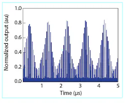
To modulate the laser, the UCLA scientists take advantage of the linear relationship between the optical loss in silicon (or the net optical gain in the laser cavity) and the free-carrier density in silicon. The linear dependence of free-carrier density on diode forward current provides direct electronic modulation of the intracavity gain. The laser is turned off when the loss induced by diode current exceeds the gain per round trip in the cavity. That is, the device functions as a “normally on” switch that is turned off when forward bias is applied to the p-n junction diode. The output pulse train of the laser can be turned off depending on the rate of carrier injection and the switching time of the diode, and turned on depending on the photon lifetime in the laser cavity. Although the team has only been able to demonstrate relatively slow modulation of 1 MHz, the modulation speed can be increased by optimizing the silicon-waveguide design and through the use of microring cavities (see Fig. 1).
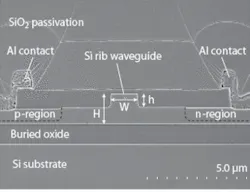
Like the UCLA silicon Raman laser, the Intel laser is constructed on a SOI substrate. But unlike the UCLA laser, which requires an external laser ring cavity, the Intel laser produces radiation entirely within an s-shaped waveguide structure on the chip. By introducing a reverse-biased p-i-n diode into the silicon waveguide, the optical loss caused by two-photon-absorption-induced free-carrier absorption is significantly reduced to the point where CW lasing can be observed (see Fig. 2).The p-i-n structure was formed by implanting boron and phosphorus in the slab on either side of the s-shaped rib waveguide, with a approximately 6-µm separation between the p- and n-doped regions. When a reverse-bias voltage is applied to the p-i-n diode, the two-photon-absorption-generated electron-hole pairs are swept out of the silicon waveguide by the electric field between the p- and n-doped regions. The effective carrier lifetime decreases with increased bias voltage to about 1 ns, compared to free-carrier lifetimes of several tens of nanoseconds for ordinary silicon-rib waveguides.
In an experiment in which the p-i-n junction was pumped by a 200-mW, 1550-nm CW external-cavity laser diode with 25‑V reverse bias, the Intel silicon laser produced more 6 µm than 8 mW of CW output power. The performance can be improved with optimization of cavity design.
The research teams plan to continue developing silicon-laser technologies. “It is an exciting time,” says Mario Paniccia, director of the Photonics Technology Laboratory at Intel.
REFERENCES
1. O. Boyraz and B. Jalali, Optics Exp. 13, 3, 796 (Feb. 7, 2005).
2. H. Rong et al., Nature 433, 725 (Feb. 17, 2005).
About the Author

Gail Overton
Senior Editor (2004-2020)
Gail has more than 30 years of engineering, marketing, product management, and editorial experience in the photonics and optical communications industry. Before joining the staff at Laser Focus World in 2004, she held many product management and product marketing roles in the fiber-optics industry, most notably at Hughes (El Segundo, CA), GTE Labs (Waltham, MA), Corning (Corning, NY), Photon Kinetics (Beaverton, OR), and Newport Corporation (Irvine, CA). During her marketing career, Gail published articles in WDM Solutions and Sensors magazine and traveled internationally to conduct product and sales training. Gail received her BS degree in physics, with an emphasis in optics, from San Diego State University in San Diego, CA in May 1986.

