Newsbreaks
320 × 256 focal-plane array uses quantum dots in a well to sense two colors
Building on an earlier demonstration of quantum-dots-in-a-well (DWELL) detectors that sense multiple wavelengths in the middle-wavelength infrared (MWIR) and in the longer-wave-infrared (LWIR) region (see Laser Focus World, December 2003, p. 9), members of the same research team from the University of New Mexico (Albuquerque, NM) and new researchers from Zia Laser (Albuquerque, NM), the University of Texas (Austin, Texas), and BAE Systems (Nashua, NH) have now demonstrated a two-color focal-plane array using a voltage-tunable DWELL detector structure.
In this DWELL structure, indium arsenide quantum dots are placed in an indium gallium arsenide well, which is then placed in a gallium arsenide matrix. A 320 × 256-pixel array is fabricated from 100-µm-aperture-diameter detector pixels on a 30-µm pitch and then bonded to a read-out integrated circuit using flip-chip technology. Thermal imaging at 80 K shows array sensitivity between 3 to 5 µm (MWIR) and 8 to 12 µm (LWIR). DWELL detectors have advantages over quantum-well IR photodetectors that include lower dark current, higher responsivity, normal-incidence detection, and improved radiation hardness. Contact Sanjay Krishna at [email protected].
Steel-ball microrubbing boosts viewing angle of liquid-crystal pixels
Many years of development in flat-panel liquid-crystal displays (LCDs) have pushed their viewing angles up from an initially small range. One approach to increase viewing angle is based on subpixel patterning techniques that orient the liquid crystal to the pixel in a way that allows each pixel to project in multiple directions. On the whole, however, these techniques (lithographic, vacuum deposition, and so on) are process-intensive. Scientists at Eindhoven University of Technology (Eindhoven, The Netherlands) have developed a simpler way to pattern LCD pixels.
In the technique, a 1-mm steel ball is pressed against the pixel’s polyimide alignment layer and, under a 150-g load, is moved back and forth several times across the pixel in displaced parallel scans of alternating direction. The process tips the aliphatic liquid-crystal-alignment chains in the polyimide along the scan directions. Although the 10-mm/min scan velocity would imply long manufacturing times, in reality a large array of balls would be scanned simultaneously across many pixels. Preliminary experimental results that include polarizing-microscope measurements on 45 × 45-µm2 pixels show the symmetric isointensity curve necessary for wide-angle viewing. Contact Soney Varghes at [email protected].
Laser diode and invisible ink turn inkjet printer into paper cutter
In a development that may have wide application in the world of consumer electronics, researchers at CEA Le Ripault (Monts, France) have created a low-cost way to endow the everyday inkjet printer with precise paper-cutting abilities. The patented approach combines a relatively low-power (on the order of a watt) single-emitter IR laser diode with an ink that is transparent to visible light but absorbent in the IR. Both the laser and the additional ink cartridge can be mounted on the print head.
The ink is formulated from a pigment called Aldrich IR 820; thin invisible lines of ink are printed on the paper in the proper places. In an experiment, a 1-W laser diode with a 100-µm emitter width was focused on the paper by two uncoated aspherical condensers, resulting in 0.8 W at the paper. For common 80-g/m2, office-grade white paper the cutting speed was 0.75 m/min; the speed scales linearly with laser power. Uses include the cutting of complex shapes that can include partially scored cuts suitable for folding; the cut-out profile of two swimmers shown here is standing upright thanks to an easily foldable scored base. Contact Olivier Acher at [email protected].
Polymer-fullerene solar cell is also electroluminescent
Researchers at Pusan National University (Pusan, South Korea) have reported the surprising result that a semiconductor polymer-fullerene composite photovoltaic (PV) material emits light when electrically stimulated. The result is surprising because the material exhibits strong photoluminescence quenching. Fullerene is a carbon (C)-based material consisting of C60 molecules, or “buckyballs.”
Solar cells with varying polymer-fullerene concentrations were fabricated and tested under 532-nm laser light. The cells showed typical PV effects. With no illumination and forward biases of up to 10 V, the cells emitted low-level but clearly visible light with spectral peaks at 600 nm and into the near-IR; luminance reached approximately 20 cd/m2 at 10 V for one device. The researchers attribute the effect to an exciplex formed between electrons in the fullerenes and holes in the polymers. Possible practical applications include displays that recharge themselves from ambient light. Contact Kwanghee Lee at [email protected].
Lithium niobate thin films improve waveguiding
Conventional waveguides in lithium niobate (LiNbO3) crystals are fabricated using metal diffusion, ion exchange, or proton exchange. Using these methods, a very small index change in the crystal is induced that causes the confinement of light to be weak and the mode size to be large, causing waveguide inefficiency and a large bending radius (a few millimeters). Recently, researchers from the University of Southern California (Los Angeles, CA) were able to fabricate submicron thin films of crystalline LiNbO3 that have a mode size less than 1 µm2 and a bending radius of a few microns.
Using crystal ion slicing and wafer bonding, LiNbO3 thin films were transferred to a substrate with a silicon dioxide cladding layer. Straight ridge waveguides were then defined using photolithography and a top layer of silicon dioxide was added before final processing. Measurements at 1550 nm for a 5-mm-long waveguide confirmed that the thin-film layers have the same optical and electro-optical properties as LiNbO3 single crystals. Contact Payam Rabiei at [email protected].
VECSEL emits two coaxial beams at different wavelengths
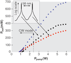
Researchers from the Optoelectronics Research Centre at the Tampere University of Technology (Tampere, Finland) have demonstrated a vertical external-cavity surface-emitting laser (VECSEL) that emits two different wavelengths simultaneously at about the same optical power from a single cavity. Pumped with a 2.4-W laser diode, the laser emits two coaxial beams at 984 and 1042 nm (figure inset shows lasing spectrum). Each beam is continuous wave (CW), single transverse mode, and greater than 100 mW in power. About 75 % of the emission can be lens-coupled into a single-mode fiber. At a higher pump power, the VECSEL self-pulsates, with sinusoidal pulse components riding on continuous-wave components. By adjusting the external cavity, a total room-temperature output of more than 1 W (though not CW) is achieved with 9-W pump power.
The laser contains eight nonidentical quantum wells placed in three different gain regions separated by potential-energy barriers to allow for dual-wavelength operation in the same cavity without mode competition and signal crosstalk. The structure was grown in a single-step process by molecular-beam epitaxy. With improvements, single-mode dual-wavelength CW optical power approaching 1 W at room temperature should be feasible. Contact Antti Härkönen at [email protected].
Bragg grating in KTP stabilizes seed laser
A lightweight and energy-efficient seed laser developed by engineers at AdvR (Bozeman, MT) is being qualified by AdvR and NASA for space flight. The laser will seed high-power solid-state lasers to eliminate fluctuations in intensity under high-power operation. In the device, the wavelength emitted from a semiconductor optical amplifier is stabilized via optical feedback from a Bragg grating in a potassium titanyl phosphate (KTP) waveguide. The compact, highly stable external-cavity laser has a single-frequency output in the range of 1047 to 1064 nm in continuous-wave or pulsed mode.
Unlike Bragg gratings in fiber, KTP has a strong birefringence that separates both reflected polarizations by several nanometers, allowing competition for laser gain from both polarizations to be eliminated by rotating the KTP waveguide to the desired polarization. This enhances the frequency stability of the laser. A version has been laboratory tested by NASA researchers at Goddard Space Flight Center (Greenbelt, MD) and has produced more than 300 billion pulses without failure. “The technology can be used to create additional narrow-bandwidth ultrastable lasers for use in spectroscopy, sensing, and communication,” says Philip Battle, AdvR’s vice president of technology. Contact Gregg Switzer at [email protected].
Triangular carbon-nanotube lattices are low in cost
To avoid costly electron-beam lithographic methods of fabricating catalyst dots for growth of carbon nanotubes, researchers at Boston College (Chestnut Hill, MA) are using low-cost self-assembly techniques to prepare triangular lattices of aligned carbon-nanotube arrays.
To fabricate the triangular lattice, self-assembled polystyrene microspheres are used as a mask over which nickel (Ni) is sputtered. Removal of the spheres and the underlying photoresist by ultrasonication leaves holes in a continuous Ni film (Ni network) upon which a second Ni layer is evaporated. The Ni in the holes adheres more strongly to the silicon substrate surface than to the previously sputtered Ni network. Another ultrasonication process removes the Ni network and leaves isolated Ni dots on the silicon substrate that are then used as catalysts to grow aligned carbon nanotubes by plasma-enhanced chemical-vapor deposition. The triangular photonic-crystal lattice has higher rotational symmetry and planar uniformity than honeycomb arrays of carbon nanotubes. Calculations show that the photonic band structure supports a negative index of refraction; by addition of dielectric materials to the internanotube spaces, subwavelength lensing can be demonstrated in simulation at visible frequencies. Contact Zhifeng Ren at [email protected].
Plasmon polaritons are guided with zero bend loss
Researchers at the Queensland University of Technology (Brisbane, Australia) have demonstrated virtually 100% transmission of channel-plasmon polaritons (CPPs) in sharp 90° bends in a subwavelength waveguide-a capability that has been previously demonstrated only for photonic-crystal waveguides, which do not provide subwavelength localization.
The subwavelength waveguide consists of a triangular groove on a silver surface. When two of these grooves or arms meet in a 90° bend, transmission of the CPP is 86%. However, if a pillar defect is introduced into the V-groove at the intersection point (with the corner of the pillar in the middle of the grooves), CPP transmission is close to 100%. Numerical calculations confirm that 100% transmission through the bend is related to destructive interference of CPPs reflected back into the first arm from the different sides of the pillar defect. This waveguiding capability is important for the development of photonic devices with levels of miniaturization and integration that are far beyond those allowed by the diffraction limit of light and dielectric waveguides. Contact Dmitri Gramotnev at [email protected].


