Silver planar lens achieves super-resolution
Researchers at the University of Canterbury (Christchurch, New Zealand) have been developing silver planar lenses that have a negative real refractive index (see Laser Focus World, July 2004, p. 11). Potential negative-refractive-index (NRI) materials include metamaterials constructed of arrays of subwavelength resonant structures (demonstrated at microwave frequencies) and thin films of certain metals (demonstrated at optical frequencies). Optics made from NRI materials can have unusual properties that include the ability of all-planar optics to form focusing systems, which is just what the silver planar lens does.
Now, the researchers have demonstrated another property predicted for certain NRI optics, called superlenses: super-resolution or resolution below the diffraction limit.1 Because the silver planar lens is a near-field device, it is not directly violating the Rayleigh (or other similar) resolution criterion, which is derived for imaging in the far field. For example, a near-field fiberoptic probe can also create spot sizes below the diffraction limit. The planar lens, however, potentially can be scaled up to create a super-resolved image of a very large area-limited, in fact, only by considerations such as mechanical feasibility, rather than constraints imposed by the optics themselves.
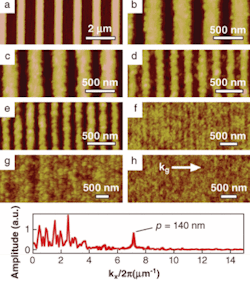
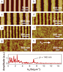
The 50-nm-thick planar silver lens is fabricated on a glass mask support containing a thin-film tungsten pattern, but is sandwiched between two layers of clear dielectric (either polymer or fused silica). The two clear layers, a few tens of nanometers in thickness, space the lens away from both the object and the image, giving the lens room to operate; the first layer also planarizes the tungsten pattern. The structure is vacuum-contacted with a photoresist- and antireflection-coated wafer; exposure with 365‑nm light creates an image in the resist. Image resolution to 170 nm was achieved. Although resolution below the 243‑nm diffraction limit was poor, the researchers claim that the fact that the lens resolved at all confirms a controversial superlensing proposal.2
Not just proximity printing
“The silver superlens work is different from simple proximity printing in one important aspect,” explains Richard Blaikie, one of the researchers. “In proximity printing, the image quality (for example, image contrast) degrades as one goes away from the object, so the best image is always formed in intimate contact, whereas with the silver superlens the image contrast is maximized at some distance below the silver (which depends on the thickness of the silver, the wavelength, and the types of dielectric spacers used). The important result of this is that a near-field optical system can then be designed with a nonzero working distance for which the imaging performance is optimized, instead of having to use intimate contact to get subwavelength resolution or trading off resolution against object-to-image separation (see figure).”
For silver, the superlensing effect is limited to wavelengths above 340 nm (corresponding to the plasma frequency for silver), for which the material has a negative real part of its dielectric constant and low loss, explains Blaikie. The longest wavelength at which it should be possible to observe superlensing in silver is limited by the need to use dielectric spacers that provide a form of impedance-matching across the silver-dielectric interface. “With appropriate high-index dielectrics (for example, semiconductors), operation at wavelengths of up to 500 nm should be possible,” he says. “Other metals should be possible (for example, gold, copper, or aluminum), but each will have its own wavelength range determined by its plasma frequency, and resolution limits determined by inherent material losses.”
The techniques can be used for imaging nonperiodic structures, says Blaike. “We have done this for isolated lines and line pairs with center-to-center spacings of less than 300 nm (that is, subwavelength),” he says. “We have focused on presenting results for periodic structures, as these give the ultimate test of resolution.”
REFERENCES
1. D. O. S. Mellvile and R. J. Blaikie, Optics Express 13(6) (March 21, 2005).
2. J. B. Pendry, Physical Rev. Lett. 85, 3966 (2000).