Silicon germanium device exhibits quantum-confined Stark effect
Researchers at Stanford University (Stanford, CA) have demonstrated an optical-modulation capability in CMOS-compatible materials that may enable fabrication of integrated all-optical devices with switching speeds on the order of 50 times faster than the current capabilities electronic logic circuits.1
Thin quantum-well structures made from traditional III-V optical materials such as gallium arsenide (GaAs) and indium phosphide (InP) can provide optical modulation bandwidths in excess of 50 GHz in micron-size devices through the quantum-confined Stark effect (QCSE). This Stark effect in a semiconductor, a key factor in high-performance telecommunication applications, essentially causes shifting of the optical absorption edge through electrically induced changes to its energy level, and thereby enables electrical modulation of the optical wavelengths that will be absorbed by the carriers of a material. The voltages required for this effect can be brought into reasonable ranges for practical devices through the quantum confinement of appropriate materials within nanometer-scale quantum-well structures.
Industry-wide efforts to develop silicon-based optics that would ultimately enable cost-effective integration of optical switching speeds into the dimensions of integrated circuitry within computer systems have been stymied in part by the fact that the QCSE in CMOS-compatible materials, such as silicon (Si) and germanium (Ge), has been either weak or lacking. The Stanford research team found, however, that even though the direct bandgap transition did not occur at the lowest energy levels, as in III-V materials, a QCSE comparable to III-V materials could be obtained from the direct band in germanium.
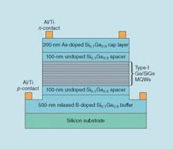
The experimental device consisted of a p-i-n diode structure (shown in cross section, but not to scale) in which strained Ge/SiGe multiple quantum wells were grown between SiGe spacers on buffer layers atop a silicon substrate. During measurements, light from a monochromator was shown down onto the top surface of the device in the open space bordered by the Al/Ti (aluminum/titanium) electrical contacts. Strong QCSE was observed at room temperature with a 4-V reverse bias over a bandwidth of 1443 to 1471 nm. At a talk given at the IEEE/LEOS 2005 Annual Meeting (Oct. 23-27; Sydney, Australia), the Stanford researchers presented their latest results, in which they produced the same effect over the telecommunications C‑band (around 1.55 mm) in redesigned germanium quantum wells.
REFERENCE
1. Y-H Kuo et al., Nature 437, 1334 (Oct. 27, 2005).
About the Author
Hassaun A. Jones-Bey
Senior Editor and Freelance Writer
Hassaun A. Jones-Bey was a senior editor and then freelance writer for Laser Focus World.
