Researchers at the Naval Research Laboratory (NRL; Washington, DC) have developed a laser direct-write technique capable of depositing particulate materials onto various substrate materials. The researchers, in collaboration with the Rochester Institute of Technology (Rochester, NY) and SFA Inc. (Largo, MD), are using this direct-write technique to deposit complex multicomponent phosphors onto both inorganic and organic substrates at 100-µm spot sizes, scalable in the future to 10 µm. The technology makes possible the construction of very-high-resolution phosphor-based displays by simple means.
A standard laser-writing technique—laser-induced forward transfer (LIFT)—can be used to transfer metallic and ceramic films of about 0.2 µm in thickness, where the absorbing medium is the metal or ceramic thin film itself. Coated on the far side of a transparent plate, the film is transferred to a proximal receiving substrate when laser radiation passes through the plate and vaporizes the film. However, although LIFT is simple, it is energetic and cannot transfer complex materials, ruling out its use for phosphors.
The process developed by the NRL researchers—matrix-assisted pulsed-laser evaporation direct write (MAPLE-DW)—can deposit complex matrices of particulate or organic material up to 30 µm thick, allowing the transfer of polymer, metallic, ceramic, and electronic materials intact. "Depending on the particulate material and the application, organics and precursors may or may not be used—many of the organics are used to selectively absorb at specific wavelengths, eliminating damage to the particulate material," says James Fitz-Gerald, one of the NRL researchers.
The output from a lasereither a krypton fluoride excimer or a frequency-tripled Nd:YAGpasses through a variable circular aperture and is focused by an ultraviolet-grade objective lens. Varying the aperture size produces beam spot sizes ranging from 10 to 300 µm. The phosphor powder to be transferred is suspended in a solution and deposited onto a gold-coated fused-silica wafer. The MAPLE-DW process is "like a laser typewriter," notes Fitz-Gerald. For this reason, the coated wafer is referred to as a ribbon. A laser dose of 0.1-2.5 J/cm2 absorbed by the gold layer transfers the phosphor to the receiving substrate. Keeping the substrate stationary produces dots; moving it results in a line.
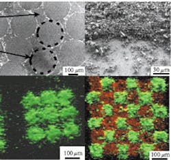
Scanning electron micrographs of the ribbon show areas of phosphor removal at low (top left) and high (top right) magnification. Optical images of a substrate show MAPLE-DW-deposited arrays of red phosphor dots (bottom left) and green phosphor dots (bottom right), both excited by 254-nm radiation. The direct-write technique is being investigated for use in the construction of cathode-ray-tube, field-emission, and electroluminescent displays, says Fitz-Gerald.
About the Author
John Wallace
Senior Technical Editor (1998-2022)
John Wallace was with Laser Focus World for nearly 25 years, retiring in late June 2022. He obtained a bachelor's degree in mechanical engineering and physics at Rutgers University and a master's in optical engineering at the University of Rochester. Before becoming an editor, John worked as an engineer at RCA, Exxon, Eastman Kodak, and GCA Corporation.

