MICROFABRICATION: One-step microjet process prints micro-optics
With demand for telecommunications components such as optical interconnects growing exponentially, various microfabrication techniques recently have left the research laboratory for the production floor. Although the techniques are not time-proven, few researchers are questioning their effectiveness. One reason is that just as a microfabrication technology proves useful in one application, another potential application often crops up, and then another, all looking to feed off a key "promised" benefit of that technique—low fabrication costs for the micro-optics.
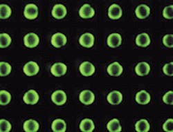
Such appears to be the case with microjet printing of micro-optical interconnects and sensors (see image). At the January 2000 Photonics West conference (San Jose, CA), researchers from MicroFab Technologies Inc. (Plano, TX) reviewed the performance of a one-step microfabrication process in producing microlens arrays for massively parallel vertical-cavity surface-emitting laser (VCSEL) based datacom switches. Another use was in depositing lenslets of various configurations onto the tips of single-mode telecom fibers. The lenslets' functions could be to collimate the output beams for free-space optical interconnection or to increase the fiber numerical aperture for collection of light from edge-emitting diode lasers.
Just as interesting, though, were two new suggested applications—fabrication of indicator-chemistry elements in arrays onto the tips of fiberoptic imaging bundles for multifunctional biochemical sensors and printing of gradient-index-of-refraction microlenses in applications requiring reduced focal spot size.
According to MicroFab researcher W. Royall Cox, the piezoelectric-based, drop-on-demand inkjet-printing technique can dispense 20-130-µm drops of optical materials at up to 10,000 drops per second onto optical substrates of arbitrary geometry at temperatures as high as 300°C.1 Materials include ultraviolet (UV) curing polymers, index-tuned thermoplastic formulations, and optical adhesives. Unlike inkjet printers that produce drops continuously and direct them to the substrate when needed by a charge-and-deflect method, the piezoelectric-based technique applies a voltage pulse only when a drop is desired. This voltage induces a volumetric change in the fluid within the printing device. The resulting pressure/velocity transients in the fluid produce the drop at the orifice of the device that is then directed onto the target substrate.
One advantage of the single-step technique over photolithographic methods is that optical epoxies used can have higher thermal durability than photoresists. The process also is flexible. By varying process parameters, such as material and drop size, the company has fabricated arrays of spherical and cylindrical plano-convex microlenses with dimensions ranging from 60 µm to several millimeters. According to Cox and colleagues Chi Guan and Donald Hayes, current hemispherical microlens printing accuracies and repeatabilities are on the order of 1% and 2% of nominal values for diameter and focal length, respectively, with relative and absolute placement accuracies near 2 and 5 µm, respectively.
Applications
In a current data-communications application, the firm is microjet-printing arrays of thousands of microlenses for use as free-space optical interconnects in massively parallel VCSEL-based photonic switches under development in conjunction with a Defense Advanced Research Projects Agency program called VCSEL-based Interconnects in VLSI Architectures for Computational Enhancement.2 Arrays are printed onto 3-in.-diameter quartz wafers in 12-group patterns, each comprising two identical 34 x 34 arrays of 300-µm-diameter 60-µm-sag microlenses.
In this application, a microlens array is aligned to a similar VCSEL-photodetector array with identically interlaced patterns of VCSELs and photodetectors. The two microlenses within each pixel area collimate the beam from a VCSEL emitter and focus a returning beam into the adjacent photodetector.
The researchers say printed microlenses were chosen for this application based on the greater coupling efficiency and wavelength independence of refractive lenslets compared to diffractive ones and the high lenslet speeds required. The optical epoxy also has a higher thermal durability than the photoresist used in photolithographically produced refractive lenslets.
Another application currently being explored is fabrication of multifunctional fiberoptic biochemical sensors. Cox explains that if the UV-curing optical epoxies are modified to provide enhanced porosity over the formulations used for microlens printing and then doped with biochemical indicators, they could be printed into a pattern of sensor elements onto the tips of imaging fiber bundles.
Cox, Guan, and Hayes also believe microjet printing could allow low-cost fabrication of gradient-index microlenses of several configurations. To their knowledge, no stand-alone microlenses with refractive-index gradients have yet been produced in either glass or optical plastic.
The inkjet-printing process they are studying uses a dual-print-head system to sequentially deposit two optical epoxies of differing refractive index at the same location to build an index gradient in the vertical direction. One possible benefit of the process could be increased performance. A ray-tracing model developed by the researchers has indicated that an axial index gradient of only 0.01 in a hemispherical lenslet with 50-µm sag has the potential to reduce focused spot size fiftyfold and to increase the Strehl ratio twenty-fivefold over a homogeneous lenslet of identical geometry.
REFERENCES
- W. R. Cox, C. Guan, and D. Hayes, Proc. Photonics West 2000, #3952B-56 (Jan. 2000).
- Y. Liu et al., Proc. Photonics West 2000, #CR76-05 (Jan. 2000).
About the Author
Paula Noaker Powell
Senior Editor, Laser Focus World
Paula Noaker Powell was a senior editor for Laser Focus World.
