NONLINEAR MATERIALS: Frequency conversion extends GaAs into mid-IR
Researchers at Stanford University (Palo Alto, CA) have demonstrated quasi-phasematched frequency conversion in 200-µm-thick gallium arsenide (GaAs) films, with the intention of facilitating nonlinear frequency conversion at wavelengths longer than the four-to-five-micron upper limit for transparency in ferro-electric materials such as lithium niobate and lithium tantalate.
In addition to taking advantage of GaAs transparency out to 12 µm and beyond, the researchers hope to benefit, primarily in potential remote-sensing applications, from the large GaAs nonlinearity (more than 90 pm/V), as well as the material's high thermal conductivity and large damage threshold.
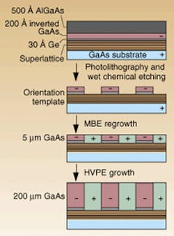
The orientation-patterned material was fabricated in a multistep process beginning with a thin layer of germanium sandwiched between two layers of GaAs (see Fig. 1). A key factor in successful fabrication entailed figuring out how to build this first sandwich layer using polar-on-nonpolar molecular beam epitaxy (MBE) instead of wafer bonding of complicated patterns, according to Loren Eyres, a member of the Stanford research team led by Martin Fejer.
"Because GaAs is lattice matched to germanium or very close to lattice matched and germanium is not polar, it allows us to grow a layer of GaAs with opposite phase on top," Eyres said. "If you were just growing GaAs and GaAs, it would always follow in registry with what was underneath it. So what you need to do is find something that's neutral basically that you can put in between, and the germanium serves very well for that." Actually working that step out took a lot of trial and error, he added. About four years elapsed between original conception of the idea and the actual successful demonstration.
After the first MBE step, an orientation template was fabricated in the material using photolithography followed by MBE regrowth. And the last step, achieving 200-µm thickness in the films, presented challenges also. "The key there was finding a growth process that simultaneously allowed the growth of thick layers and preserved the [vertical] fidelity of the domains up through those thick layers," Eyres said. This step was achieved through a collaboration with researchers at Thomson-CSF (Orsay, France) who used hydride vapor-phase epitaxy (HPVE) to grow the thick vertical films (see Fig. 2).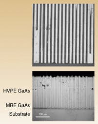
A primary consideration in moving the GaAs films beyond the laboratory and into actual commercial applications will be to increase the thickness of the films. "What we've demonstrated so far is 200 µm, and the range of thickness that people would like to see is around 500 µm," Eyres said. "At that point it begins to be something people would consider using. That's the thickness at which lithium niobate became useful."
While pointing out that a good bit more development will be required before the technique is likely to produce devices for commercial applications, Eyres also argues the significance of the scientific achievement in and of itself. "It's important because we know that you can grow a thick GaAs film with these beautiful vertical domain boundaries," he said. "We don't understand all of the reasons why it grows that way versus growing on a different plane or direction for example. But the proof that it works motivates [additional] research to understand how to take care of the rest of the problems."
About the Author
Hassaun A. Jones-Bey
Senior Editor and Freelance Writer
Hassaun A. Jones-Bey was a senior editor and then freelance writer for Laser Focus World.