Electron Optics: Megavolt microscope sees 50-pm features
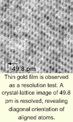
TOKYOKoichi Kitazawa and colleagues at the University of Tokyo have completed a 1-MV electron interference microscope and succeeded in resolving a crystal lattice with a 49.8-pm period, a record in the field (see image on p. 46). Development of this electron microscope was conducted at Core Research for Evolutional Science and Technology (CREST), an organization sponsored by the Japan Science and Technology Corp. (Kawaguchi). The goal was to develop high-quality spatial resolution of the phase and amplitude of electron waves. The work is a collaboration between the University of Tokyo and Hitachi Ltd.
Electron-interference microscopy incorporates a field-emission electron gun and an electron-wave interference device. This device is used to separate an electron wave into two components, which are then recombined after being given different directions. Because electrons have wavelike properties, interference bands are thus formed. Electron waves are distorted by electromagnetic fields in and around the sample, causing the relative phase to change, a phenomenon observed as distortion in the interference bands.
To improve the resolution of such microscopes, the wavelength of the electrons must be decreased. The electrons consequently must be accelerated across very high voltages; however, it is difficult to operate a megavolt field-emission electron gun under stable conditions. To remedy this problem, the electron accelerator tube and gun, the power source to control the gun, and the high-voltage production apparatus had to be separated and connected using high-voltage cables. By separating the components, electromagnetic noise emitted from the power source was blocked from the electron gun. To further reduce noise, high-voltage cables, filter resistors, and filter condensers were used. As a result, a stability of 0.5 V/min could be achieved per 1-MV acceleration voltage. In addition, the vibration of the electron source was decreased to one-tenth of the height of the electron source by increasing the rigidity of each component. Finally, by optimizing the electron optics, luminance was increased to 1.8 x 10¹⁰ A/cm2-sr.
Electrons entering the crystal are diffracted by the ordered atoms so that they emerge separated into many waves. Electron microscopes collect these waves using electron lenses to form an image. By using the diffracted waves to form the image, crystal lattice images are seen, because they are simply collections of interference bands. The separation between bands corresponds to the separation between atom surfaces, so it has been used as a control for resolution. By using a different technique called Lorentz microscopy, the behavior of magnetic flux particles within high-temperature superconductors can be observeda measurement that has up until now been hindered by the thickness of the sample.
Courtesy O plus E magazine, Tokyo

